Download presentation
Presentation is loading. Please wait.

1
Is Graphene ending the promises for Carbon Nanotubes? Posted on June 12th, 2013 at 12:20 pm by Krisztián Niesz from Chem Axon

2
Carbon Materials Fullerene Tubes Cones Carbon black Horns Rods Foams Nanodiamonds

3
From Chemaxon Let me start with what’s in the background, and why I think this is a valid and potentially a highly influential technological issue these days. This month it rather surprisingly hit the news that three years after Bayer MaterialScience (a leader in material solutions) invested 22 million euros into a carbon nanotube (CNT) production facility which had a very promising future, then they decided to close it down because of lacking groundbreaking applications in sight. 1 In other words they trusted, somewhat blindly, that the growth rate of worldwide CNT demand could increase up to the level of the production capacity. Well, as you’d guess this is still very much unbalanced toward the latter. Or, is it the success of the Nobel Prize-winning big brother – graphene – that is shaking the whole CNT empire? When Sumio Iijima discovered nanotubes in 1991 the future looked particularly bright for this novel carbon allotrope, holding potential applications in several industrial sectors, such as coatings, electronics, composites and energy storage. Yet more than 20 years after that famous Nature paper 2 it is only the application as a reinforcing material in plastics and composites that was somewhat able to meet the expectation. 2013 started with dozens of companies producing several thousands of metric tons of multiwall nanotubes a year, but only one month in the new year the production decreased by around 10% as a result of Bayer MaterialScience leaving the business. The circle of the remaining big players still includes companies such as the Japanese Showa Denko K.K. (recently partnered up with Mitsubishi, and mainly producing vapor grown carbon fiber VGCFTM), Nanocyl (spun off from the University of Namur in early 2000s) and the US-based CNano Technology Ltd., Arkema Inc. and Hyperion Catalysis, all with annual capacities of several hundreds of metric tons. In contrast to CNTs, graphene in the past few years has been developing at an astonishingly high rate, both in the area of applications and production. It is often called as the next disruptive technology representing unique and highly attractive electrical, optical and mechanical properties. 3 Although it is very similar to carbon nanotubes (essentially a single wall nanotube is a rolled up graphene sheet), it is much easier to make. So there is one advantage already, and the industry is currently facing an annual production capacity of 1,000s of metric tons in China alone. Targeting the same sectors as CNTs, but developing at a much faster rate would easily mean that graphene is going to take over the market from nanotubes and/or create its own market. Maybe this was the issue that has been realized by the management of Bayer MaterialScience, and has led to the decision of leaving a market currently estimated to worth around 600-700 million dollars. We don’t know yet, but that is very likely to be the case. It is a bit too early to predict the outcome of this battle, but in my opinion other leading companies might as well follow the example setup by Bayer MaterialScience, and in turn the applications of CNTs could fairly easily shrink down to the currently existing composites, or, in time even vanish completely. This won’t be just caused by a global meltdown that has set back the worldwide demand for carbon nanotubes considerably during the years 2008 and 2009, rather an evolutionary thing that allows similar technologies to jump across one another.
 invested 22 million euros into a carbon nanotube (CNT) production facility which had a very promising future, then they decided to close it down because of lacking groundbreaking applications in sight. 1 In other words they trusted, somewhat blindly, that the growth rate of worldwide CNT demand could increase up to the level of the production capacity. Well, as you’d guess this is still very much unbalanced toward the latter. Or, is it the success of the Nobel Prize-winning big brother – graphene – that is shaking the whole CNT empire. When Sumio Iijima discovered nanotubes in 1991 the future looked particularly bright for this novel carbon allotrope, holding potential applications in several industrial sectors, such as coatings, electronics, composites and energy storage. Yet more than 20 years after that famous Nature paper 2 it is only the application as a reinforcing material in plastics and composites that was somewhat able to meet the expectation started with dozens of companies producing several thousands of metric tons of multiwall nanotubes a year, but only one month in the new year the production decreased by around 10% as a result of Bayer MaterialScience leaving the business. The circle of the remaining big players still includes companies such as the Japanese Showa Denko K.K. (recently partnered up with Mitsubishi, and mainly producing vapor grown carbon fiber VGCFTM), Nanocyl (spun off from the University of Namur in early 2000s) and the US-based CNano Technology Ltd., Arkema Inc. and Hyperion Catalysis, all with annual capacities of several hundreds of metric tons. In contrast to CNTs, graphene in the past few years has been developing at an astonishingly high rate, both in the area of applications and production. It is often called as the next disruptive technology representing unique and highly attractive electrical, optical and mechanical properties. 3 Although it is very similar to carbon nanotubes (essentially a single wall nanotube is a rolled up graphene sheet), it is much easier to make. So there is one advantage already, and the industry is currently facing an annual production capacity of 1,000s of metric tons in China alone. Targeting the same sectors as CNTs, but developing at a much faster rate would easily mean that graphene is going to take over the market from nanotubes and/or create its own market. Maybe this was the issue that has been realized by the management of Bayer MaterialScience, and has led to the decision of leaving a market currently estimated to worth around million dollars. We don’t know yet, but that is very likely to be the case. It is a bit too early to predict the outcome of this battle, but in my opinion other leading companies might as well follow the example setup by Bayer MaterialScience, and in turn the applications of CNTs could fairly easily shrink down to the currently existing composites, or, in time even vanish completely. This won’t be just caused by a global meltdown that has set back the worldwide demand for carbon nanotubes considerably during the years 2008 and 2009, rather an evolutionary thing that allows similar technologies to jump across one another..")
4
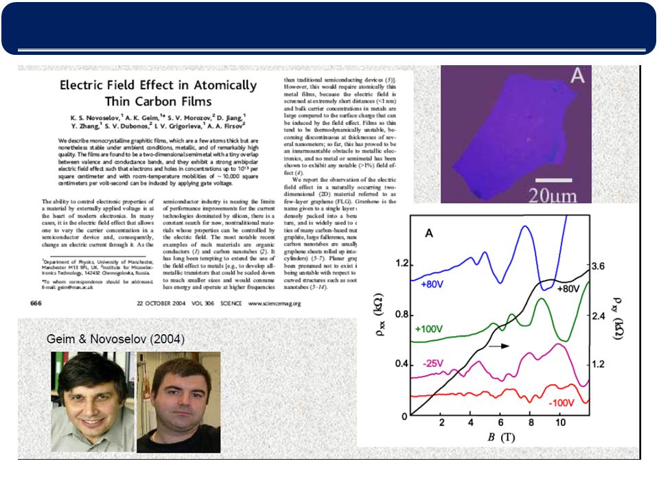
Iijima’s First Paper on CNT from 1991: Citation : 21170 Novoselov’s First paper on Graphene from 2004: Citation: 11401

5
년도별 인용 추이 Blue: CNT Red: Graphene

6
Nanotube 탄소동소체로서 하나의 탄소가 다른 탄소 원자와 육각형 벌집 무늬로 결합되어 튜브 형태를 이루고 있는 물질 하나의 탄소 원자는 3 개의 다른 원자와 sp2 결합의 육각형 벌집 구조 튜브의 직경이 대략 수 nm 정도로 극히 작기 때문에 나노 튜브라고 함 전기가 잘 통하고 열을 잘 발산시켜 안정된데다 강도와 탄성이 뛰어난 꿈의 신소재인 셈 저항 없이 전기를 흐르게 하는 초전도현상을 보이거나 반도체 성질을 가지는 등 다양한 기능을 지녀 전자소자, 정밀기계, 광소자 등 차세대 나노제품에 필수적인 ‘ 꿈의 소재 ’ 로 불리고 있다.

7
Various structures of CNT (8,8) (10,0) (8,3) m=n: Armchair n=0: Zigzag Others: Chiral 전기 전도체반도체 Single Wall Nanotube 단일벽 나노튜브 Multi Wall Nanotube 다중벽 나노튜브 Rope Wall Nanotube 다발형 나노튜브 전기 방전법 (Arc Discharge) 레이저 증착법 (Laser Vaporization) 플라즈마 화학 기상 증착법 (Plasma Enhanced CVD) 열 화학 기상 증착법 (Thermal CVD) 기상 합성법 (Vapor Phase Growth) 전기 분해 방법 Flame 합성 방법
 (10,0) (8,3) m=n: Armchair n=0: Zigzag Others: Chiral 전기 전도체반도체 Single Wall Nanotube 단일벽 나노튜브 Multi Wall Nanotube 다중벽 나노튜브 Rope Wall Nanotube 다발형 나노튜브 전기 방전법 (Arc Discharge) 레이저 증착법 (Laser Vaporization) 플라즈마 화학 기상 증착법 (Plasma Enhanced CVD) 열 화학 기상 증착법 (Thermal CVD) 기상 합성법 (Vapor Phase Growth) 전기 분해 방법 Flame 합성 방법")
8
전기 방전법 (Arc Discharge) 양극에서 기화된 탄소 클러스터들이 다른 전극인 음극에서 증착되는 과정
 양극에서 기화된 탄소 클러스터들이 다른 전극인 음극에서 증착되는 과정")
9
레이저 증착법 (Laser Vaporization / Ablation) MWNTSWNT
 MWNTSWNT")
10
Carbon Nanotube 응용분야비고 발광특성 - 저전압에서 고전자밀도 발광 -(1 ~ 3V/ ㎛ 의 동작개시전압 및 내구성 우수 ) - 고종횡비 (high aspect ratio) 고성능 전자총, FED- Mo tip :50 ~ 100V/ ㎛ turn-on 전압 크기 - 초미세크기 (0.6 ~ 1.8nm 직경 ) - 도체 및 반도체 성질 나노소자, 단전자소자, 양자소자 - EBL( 전자빔 ) 선폭구현 : ~ 50nm 형상 탄성 -Nano scale wire 또는 tip 형상 - 탄성우수 ( 휨후복원시 손상이 없음 ) 1.09TPa AFM, STM, NEMS( 나노 파이프, 피펫, 도선 ) - 금속 / 탄소섬유는 입계에서 휘어 짐 구조 - 속이 빈 공간구조, 표면적이 넓음수소저장전지, 연료전지, 모세관현상 응용, 가스센 서 - 질량기준으로 6.5% 이상되어야 전류밀도 열전도도 - 고전류밀도 ( 최대 1x10 9 A/cm2), - 고열전도도 (6000[W/(mK)]) 전자부품, 집적회로내의 도선 - 구리선전류밀도 : 최대 1x10 6 A/cm2 - 다이아몬드열전도도 : 3320W/(mK) 밀도 인장강도 내열성 - 1.33 ~ 1.40 g/cm3 가볍고 길이 방향으 로 매우 질기고 단단함 - 고강도합금의 10 배 이상 4.5x10 10 Pa - 안정성 ( 진공에서 2800 ℃ 대기중 750 ℃ ) - Al 밀도 : 2.7 g/cm3 - 고강도합금인장강도 : 2x10 9 Pa - LSI 내에서의 금속선 : 600 ~ 1000 ℃에서 녹음 CNT 의 다양한 특성과 응용분야
![Carbon Nanotube 응용분야비고 발광특성 - 저전압에서 고전자밀도 발광 -(1 ~ 3V/ ㎛ 의 동작개시전압 및 내구성 우수 ) - 고종횡비 (high aspect ratio) 고성능 전자총, FED- Mo tip :50 ~ 100V/ ㎛ turn-on 전압 크기 - 초미세크기 (0.6 ~ 1.8nm 직경 ) - 도체 및 반도체 성질 나노소자, 단전자소자, 양자소자 - EBL( 전자빔 ) 선폭구현 : ~ 50nm 형상 탄성 -Nano scale wire 또는 tip 형상 - 탄성우수 ( 휨후복원시 손상이 없음 ) 1.09TPa AFM, STM, NEMS( 나노 파이프, 피펫, 도선 ) - 금속 / 탄소섬유는 입계에서 휘어 짐 구조 - 속이 빈 공간구조, 표면적이 넓음수소저장전지, 연료전지, 모세관현상 응용, 가스센 서 - 질량기준으로 6.5% 이상되어야 전류밀도 열전도도 - 고전류밀도 ( 최대 1x10 9 A/cm2), - 고열전도도 (6000[W/(mK)]) 전자부품, 집적회로내의 도선 - 구리선전류밀도 : 최대 1x10 6 A/cm2 - 다이아몬드열전도도 : 3320W/(mK) 밀도 인장강도 내열성 ~ 1.40 g/cm3 가볍고 길이 방향으 로 매우 질기고 단단함 - 고강도합금의 10 배 이상 4.5x10 10 Pa - 안정성 ( 진공에서 2800 ℃ 대기중 750 ℃ ) - Al 밀도 : 2.7 g/cm3 - 고강도합금인장강도 : 2x10 9 Pa - LSI 내에서의 금속선 : 600 ~ 1000 ℃에서 녹음 CNT 의 다양한 특성과 응용분야](http://images.slidesplayer.org/39/11012692/slides/slide_10.jpg "Carbon Nanotube 응용분야비고 발광특성 - 저전압에서 고전자밀도 발광 -(1 ~ 3V/ ㎛ 의 동작개시전압 및 내구성 우수 ) - 고종횡비 (high aspect ratio) 고성능 전자총, FED- Mo tip :50 ~ 100V/ ㎛ turn-on 전압 크기 - 초미세크기 (0.6 ~ 1.8nm 직경 ) - 도체 및 반도체 성질 나노소자, 단전자소자, 양자소자 - EBL( 전자빔 ) 선폭구현 : ~ 50nm 형상 탄성 -Nano scale wire 또는 tip 형상 - 탄성우수 ( 휨후복원시 손상이 없음 ) 1.09TPa AFM, STM, NEMS( 나노 파이프, 피펫, 도선 ) - 금속 / 탄소섬유는 입계에서 휘어 짐 구조 - 속이 빈 공간구조, 표면적이 넓음수소저장전지, 연료전지, 모세관현상 응용, 가스센 서 - 질량기준으로 6.5% 이상되어야 전류밀도 열전도도 - 고전류밀도 ( 최대 1x10 9 A/cm2), - 고열전도도 (6000[W/(mK)]) 전자부품, 집적회로내의 도선 - 구리선전류밀도 : 최대 1x10 6 A/cm2 - 다이아몬드열전도도 : 3320W/(mK) 밀도 인장강도 내열성 ~ 1.40 g/cm3 가볍고 길이 방향으 로 매우 질기고 단단함 - 고강도합금의 10 배 이상 4.5x10 10 Pa - 안정성 ( 진공에서 2800 ℃ 대기중 750 ℃ ) - Al 밀도 : 2.7 g/cm3 - 고강도합금인장강도 : 2x10 9 Pa - LSI 내에서의 금속선 : 600 ~ 1000 ℃에서 녹음 CNT 의 다양한 특성과 응용분야")
11
응용분야 및 이슈 가격 !! 생산분산정제 대량생산 분리공정 분산의 이슈 가격 책정 경쟁 물질

12
뭐든지 잘 흡수하기 때문에 레이더 파까지 흡수 감시망에 걸리지 않는 비행기 도료로 개발하려는 움직임 가격, 분산 이슈가 아직도 존재 CNT 기반 복합체

13
AFM tips-Mechanical Properties Carbon nanotubes as AFM probe tips Small diameter – maximum resolution 1.Excellent chemical and mechanical robustness 2.High aspect ratio Resolution of ~ 12nm is achieved 인장력 및 압축력은 큼 탄성우수 E : 1.09TPa 복원이 쉽다

14
CNT 기반 Transistor 초미세소자 구현 가능 / 선 폭이 대략 nm 단위 수 nm 크기의 기억소자나 회로제작시 현재 최첨단 IC 선 폭의 1/100 정도 넓이는 1/10000 이므로 현재보다 만배 정도 집적도가 높은 칩 생산가능 기억소자로 그 집적도는 테라 (1012 즉 1 조 ) DRAM 에 이름 기존 트랜지스터에 비해 더욱 빠르게 동작 (1 테라 Hz 의 클럭 속도 예상 ) 문제점 – 대량생산요원 (Process 의 문제 ) 튜브의 배열 기술 어려움 – 새로운 응용가능성 → 뒤엉킨 상태 그대로 놓고 소위 병렬 분산 기어소자로 활용 –CNT 분리 공정 문제 !! 즉 수반되는 가격의 문제 carbon nano tube Insulator Field Effect Transistor,FET

15
Carbon Nanohorn Fuel Cell Electrodes CNT 기반 Cell Electrode Energy 분야의 연구는 가격에 대한 고려가 필수 불가결함 이외에 다른 중요한 변수들이 산재함 Catalyst Supporter 로만 사용하기에는 아직까지는 가격이 높음

16
Yarn Zhang, Atkinson and Baughman, Science 306 (2004) 1358. MWCNT Operational -196 o C < T < 450 o C Electrical conducting Toughness comparable to Kevlar

17
Biological applications: DNA sequencing Nanotube fits into the major grove of the DNA strand Apply bias voltage across CNT, different DNA base-pairs give rise to different current signals With multiple CNT, it is possible to do parallel fast DNA sequencing Top view and side view of the assembled CNT-DNA system Graphene 으로는 성공할 수 없는 몇 개의 응용 분야 CNT 에 대한 생물학적 안정성 ? 분산의 문제 다양한 Nano-Medical (i.e Drug Delivery, or Biosensor) 에서의 응용 가능성이 남아 있음
 에서의 응용 가능성이 남아 있음.")
18
Nanofluid 나노유체 (Nanofluid) - 나노입자가 균일하게 분산된 열전달 유체 - 일반적으로 고체 입자는 액체에 비해 열전달 특성이 우수 - 나노입자의 평균 크기 : 1~100 nm 열전달 나노유체 열전달 유체 S. U. S. Choi et al. Anomalous thermal conductivity enhancement in nanotube suspensions Appl. Phys. Lett. 2001, 79, 2252.

19
CNT Hydrogen adsorption CNT 를 2 차전지 전극 및 연료 전지에 응용가능 내부가 비어 있고, 표면적이 넓은 특징을 이용, 빈 공간에 수소를 저장 낮은 밀도, 큰 저장공간으로 단위 질량 당 전하저장 능력 우수 관 속에 수소를 저장해 배터리로 쓰거나 고순도 정화필터로 활용가능 요구되는 연료전지의 수소저장효율은 6.5 %, 62 kg / m 3 ( 상온, 상압 ) – 미국 에너지성 (DOE) 목표 : 전기자동차 500 km 주행 기준 많은 종류의 CNT 들이 2 %, 6 % 그리고 20 % 이상의 효율 가지기도 – 이유 : 물리화학적 흡착력, 활성화 에너지 대략 90 kJ /mole tank H2H2 P, T ?
 – 미국 에너지성 (DOE) 목표 : 전기자동차 500 km 주행 기준 많은 종류의 CNT 들이 2 %, 6 % 그리고 20 % 이상의 효율 가지기도 – 이유 : 물리화학적 흡착력, 활성화 에너지 대략 90 kJ /mole tank H2H2 P, T")
20
Field Emission Display ( 전계 방출표시 소자 ) 음극판에서 방출된 전자가 양극판의 형광체에 부딪혀 영상을 나타냄 각종 소자들이 1cm 이하의 얇은 진공 상태의 패널 안에 구성 핵심 기술은 emitter tip 의 가공과 안정성 기존의 실리콘 팁, 몰리브덴 팁은 수명과 안정성에 큰 문제 수명, 안정성, 전자 방출 효과가 좋은 탄소 나노 튜브 방출기를 사용 높은 가능성, But LED 및 OLED 시장이 너무 활성화됨 Samsung display 1999 (4.5inch)
 음극판에서 방출된 전자가 양극판의 형광체에 부딪혀 영상을 나타냄 각종 소자들이 1cm 이하의 얇은 진공 상태의 패널 안에 구성 핵심 기술은 emitter tip 의 가공과 안정성 기존의 실리콘 팁, 몰리브덴 팁은 수명과 안정성에 큰 문제 수명, 안정성, 전자 방출 효과가 좋은 탄소 나노 튜브 방출기를 사용 높은 가능성, But LED 및 OLED 시장이 너무 활성화됨 Samsung display 1999 (4.5inch)")
21
Pictures from http://www.space.com/businesstechnology/technology/space_elevator_020327- 1.htmlhttp://www.space.com/businesstechnology/technology/space_elevator_020327- 1.html The Space Elevator

24
Graphene is a one-atom-thick planar sheet of sp 2 -bonded carbon atoms that are densely packed in a honeycomb crystal latticesp 2 -bondedcarbon The name ‘graphene’ comes from graphite + -ene = graphenegraphite-ene High resolution transmission electron microscope images (TEM) of graphene Introduction to graphene Molecular structure of graphene A. K. Geim & K. S. Novoselov. The rise of graphene. Nature Materials Vol. 6,183-191 (2007).
..")
25
Electronic properties Optical Properties Membrane Properties Mechanical Properties Properties of graphene Optical properties

26
Graphene vs (scaled down) steel film of the same thickness => Graphene is more than 100 times stronger than the strongest steel! Take-home message 5 [Can put a 4Kg mass (e.g. a cat) on a 1 m2 graphene (if one can make it). Cartoon taken from Nobel Prize announcement] Mechanical Property - High Young’s modulus (~1,100 Gpa) High fracture strength (125 Gpa) - Graphene is as the strongest material ever measured, some 200 times stronger than structural steel
 on a 1 m2 graphene (if one can make it). Cartoon taken from Nobel Prize announcement] Mechanical Property - High Young’s modulus (~1,100 Gpa) High fracture strength (125 Gpa) - Graphene is as the strongest material ever measured, some 200 times stronger than structural steel.")
27
Chemical Property: Impermeable Membrane Not permeable even for proton! Graphene Balloon (McEuen group, 2009) Graphene Bubbles (P Kim, Columbia group, 2009)
 Graphene Bubbles (P Kim, Columbia group, 2009).")
28
Electrical Properties Graphene has unusual energy bands The p z electrons (2 in each hexagon) completely fill the lower band. The upper band is empty. One can introduce (or take away) electrons into the upper (lower) band by various methods. Electrically Conductors
 electrons into the upper (lower) band by various methods. Electrically Conductors.")
29
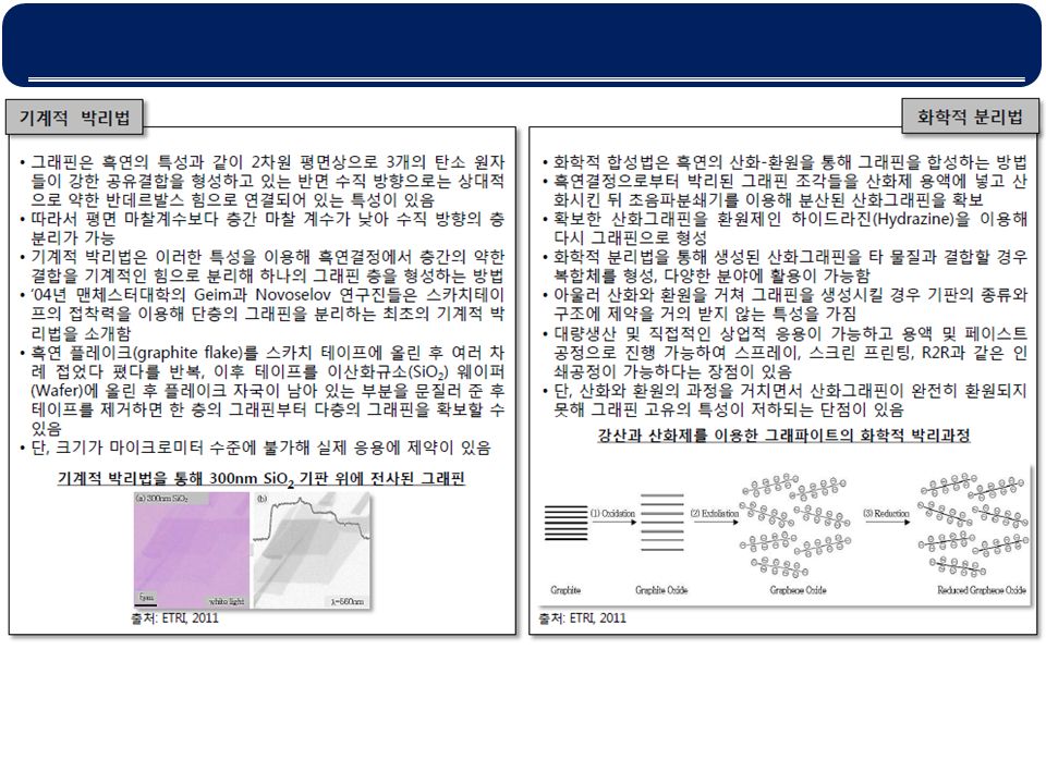
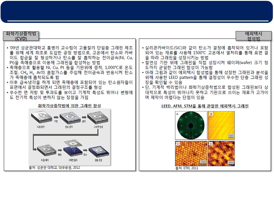
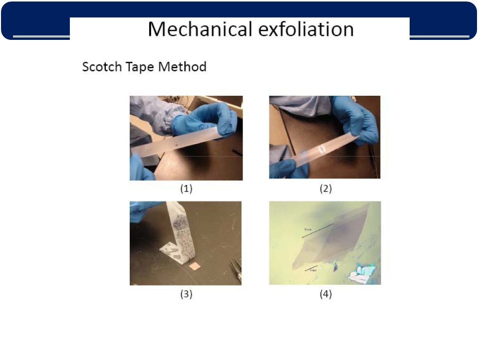
Preparation and characterization graphene Preparation methods Top-down approach (From graphite) Bottom up approach (from carbon precursors) - By chemical vapour deposition (CVD) of hydrocarbon - By epitaxial growth on electrically insulating surfaces such as SiC - Total Organic Synthesis - Micromechanical exfoliation of graphite (Scotch tape or peel-off method) - Creation of colloidal suspensions from graphite oxide or graphite intercalation compounds (GICs ) Ref: Carbon, 4 8, 2 1 2 7 –2 1 5 0 ( 2 0 1 0 )
 Bottom up approach (from carbon precursors) - By chemical vapour deposition (CVD) of hydrocarbon - By epitaxial growth on electrically insulating surfaces such as SiC - Total Organic Synthesis - Micromechanical exfoliation of graphite (Scotch tape or peel-off method) - Creation of colloidal suspensions from graphite oxide or graphite intercalation compounds (GICs ) Ref: Carbon, 4 8, – ( )")
33
J. Mater. Chem. 2005, 15, 974. Graphite intercalation compound

34
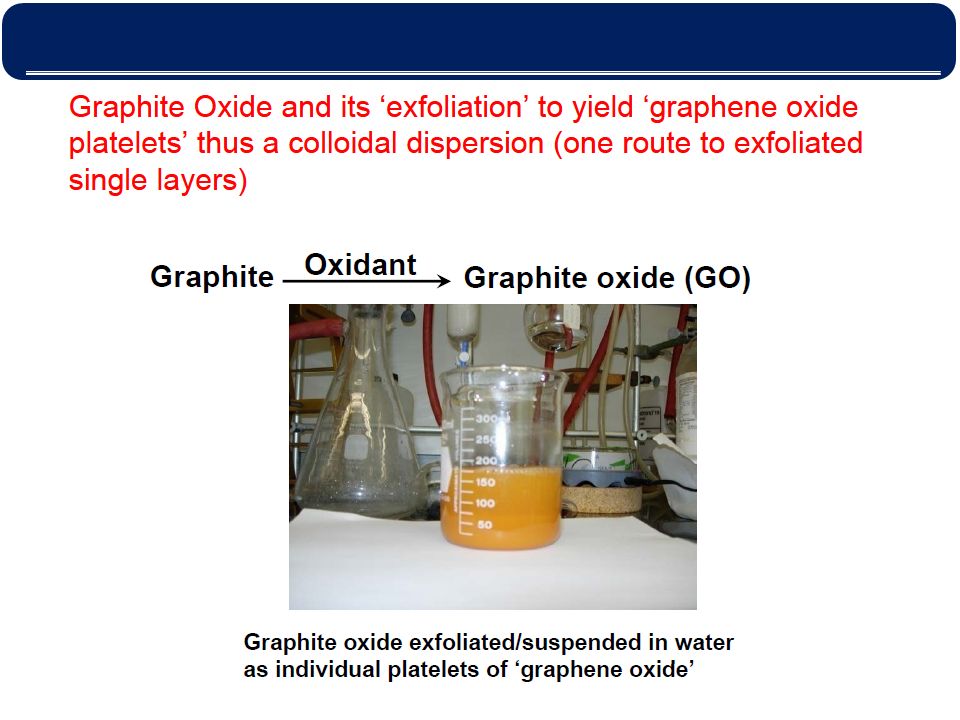
Graphite oxide method ( Most common and high yield method) Graphite Oxidation (Hummers’method) H 2 SO 4 / KMnO 4 H 2 SO 4 /KClO 3 Or H2SO 4 /HNO 3 ………………. H2OH2O Ultrasonication (exfoliation) Graphite Oxide Graphene Oxide monolayer or few layers Fuctionalization (for better dispersion ) Making composite with polymers Chemical reduction to restore graphitic structures
 Graphite Oxide Graphene Oxide monolayer or few layers Fuctionalization (for better dispersion ) Making composite with polymers Chemical reduction to restore graphitic structures.")
35
Tung, V. C., Allen, M. J., Yang, Y. & Kaner, R. B. High-throughput solution processing of large-scale graphene. Nature Nanotech. 4, 25–29 (2008). Graphite oxide method
. Graphite oxide method.")
37
More intercalation for better exfoliation to monolayers Graphite oxide Graphite oxide method

40
Yang, X. Y.; Dou, X.; Rouhanipour, A.; Zhi, L. J.; Rader, H. J.; Mullen, K. J. Am. Chem. Soc. 2008, 130, 4216. Total Organic Synthesis

41
Graphene nanoribbons (from carbon nanotube) NATURE, Vol, 458, 16, April (2009)
 NATURE, Vol, 458, 16, April (2009)")
42
Transparent, conducting and flexible electrodes K. S. Kim et al., Nature, 457, 706 (2009) Transparent, Flexible Electrode!! 다양한 응용가능성 Flexible 시대의 중요 물질로 부각될 가능성 ! 가격, Patterning, 성능
 Transparent, Flexible Electrode!. 다양한 응용가능성 Flexible 시대의 중요 물질로 부각될 가능성 . 가격, Patterning, 성능.")
43
Graphene based transistor Band-Gap Tuning 가장 큰 이슈

45
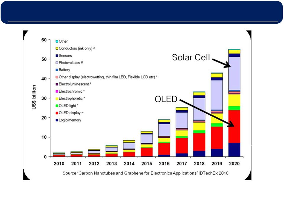
현재까지 Graphene 의 제조에 대한 연구가 다수 진행됨 CNT 로 시도된 다양한 응용 분야에 대한 연구가 기하급수적으로 증가 ( 예, Sensor, 전극물질, 바이오 응용, Transistor, Thermal Conductivity 등등 ) 더불어 CNT 응용 분야 이외의 산업적으로 매우 응용가치가 높은 분야에 대한 연구가 진행됨 ( 예, Flexible Display, Membrane Applications 등등 ) Band Gap Tuning Production! (with good quality, low price, reasonable amounts) Patterning Issue! 내스크래치성
 Patterning Issue. 내스크래치성.")
46
Final Conclusion (Personal Opinion)
")
Similar presentations


. Carbon nanotube( 탄소 나노튜브 ) Multi-walled carbon nanotube.>")


 멀티스케일 에너지 시스템 연구단은 나노기술과 에너지 기술의 융합을 통하여 혁신적 미래 광에너지와 분자에너지 원천기술 개발을 목표로 하는 멀티스 케일 에너지 시스템 연구사업을 추진하고 있습니다. 연구단에서는 격주로 멀티스케일 에너지.>")
 The negative side of the bias voltage push the free electrons in the n-regio n toward pn junction Also provide a.>")


