Download presentation
Presentation is loading. Please wait.

1
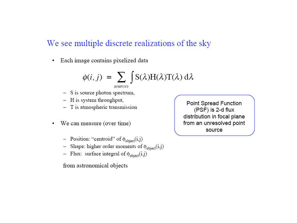
검출기 눈, 사진, Photoelectric device, Photomultipliers, Image intensifiers, Charged Coupled Device,

2
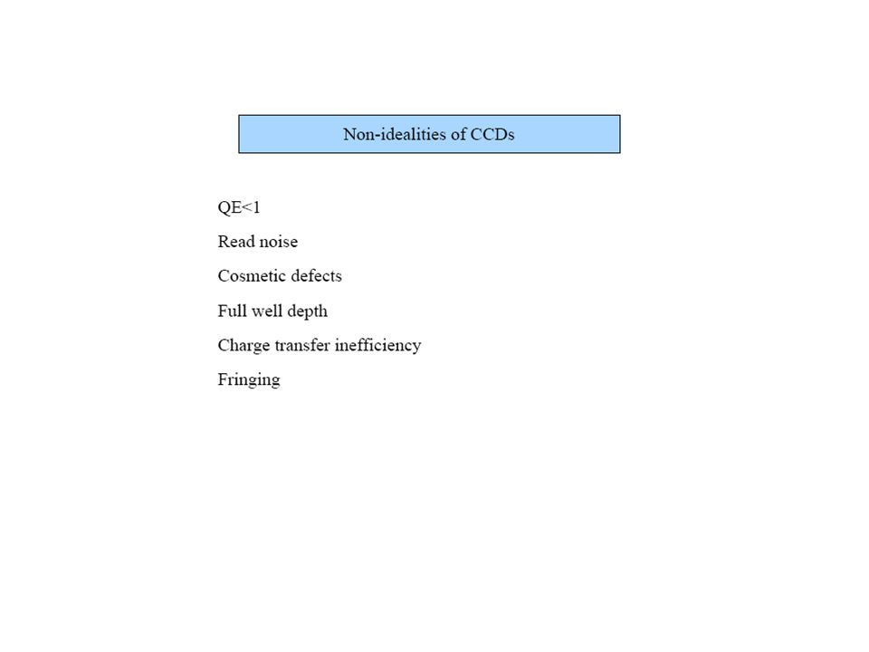
Charged Coupled Device 장점 : 1. 높은 양자효율 (60-80%) ( 사진 :2-10%, PMT: 20-40%) 2. 선형 반응 ( 사진 = 특성곡선 ) 3. digital 정보 ( 사진 = 아날로그 ) 콤퓨터 영상처리 4. 이차원 : 측광 및 측성 (PMT = 측광 only) 5. 넓은 다이나마익 범위 > 10 등급 이상 ( 사진 =5 등급 ) 6. 넓은 파장 영역에 반응 ( 사진 = 특수처리 spectral sensitization) 단점 : 1. 좁은 시야 ( 망원경시야 >> CCD 에 의해 제한된 시야 ) 2. 엄청난 자료 (512*512 CCD = 262,144 pixels, 4K*4K = 4096*4096 = 16,777,216 pixels) 3. 각 pixel 의 다른 반응 : flat 보정 필수 4. readout 잡음 관측된 자료를 읽어 올 때 발생 5. RN 잡음을 포함한 잡음을 줄이기 위한 냉각 (-100 도 C ) 필수
 3. digital 정보 ( 사진 = 아날로그 ) 콤퓨터 영상처리 4. 이차원 : 측광 및 측성 (PMT = 측광 only) 5. 넓은 다이나마익 범위 > 10 등급 이상 ( 사진 =5 등급 ) 6. 넓은 파장 영역에 반응 ( 사진 = 특수처리 spectral sensitization) 단점 : 1. 좁은 시야 ( 망원경시야 >> CCD 에 의해 제한된 시야 ) 2. 엄청난 자료 (512*512 CCD = 262,144 pixels, 4K*4K = 4096*4096 = 16,777,216 pixels) 3. 각 pixel 의 다른 반응 : flat 보정 필수 4. readout 잡음 관측된 자료를 읽어 올 때 발생 5. RN 잡음을 포함한 잡음을 줄이기 위한 냉각 (-100 도 C ) 필수.")
3
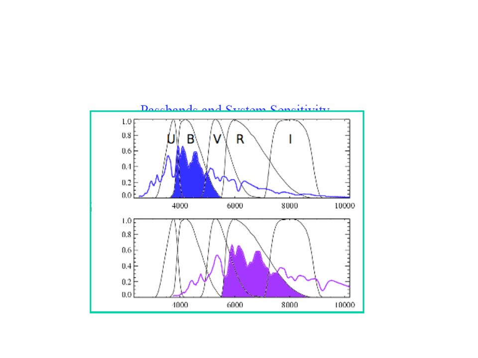
검출기들의 양자효율

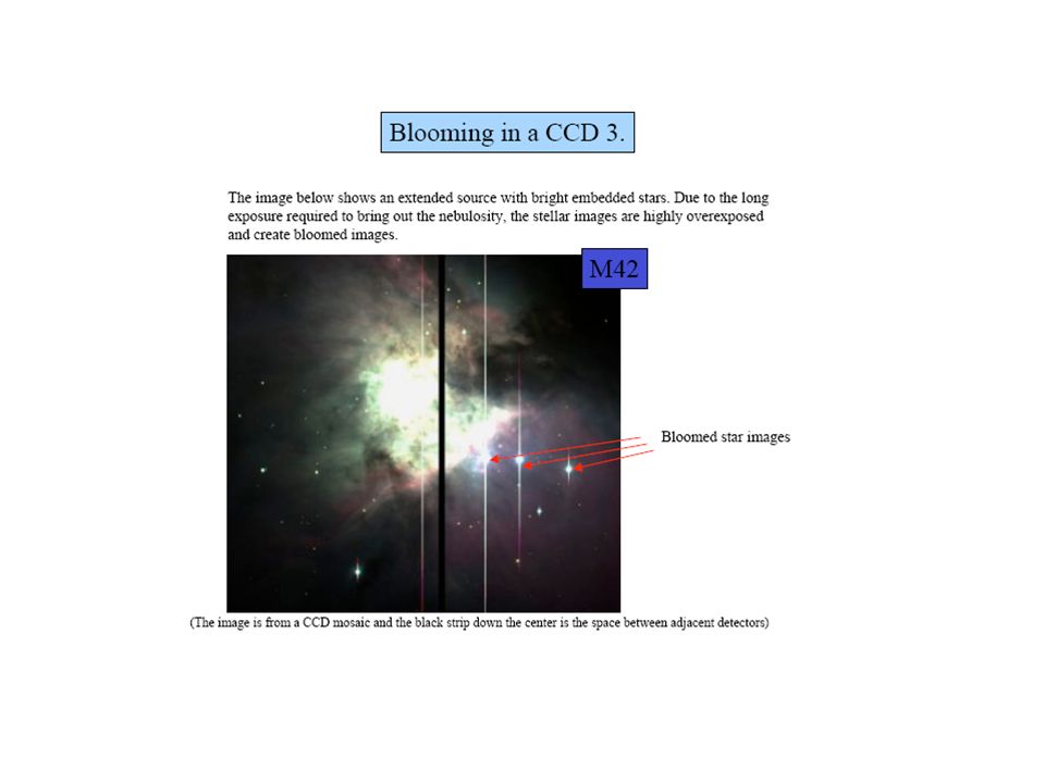
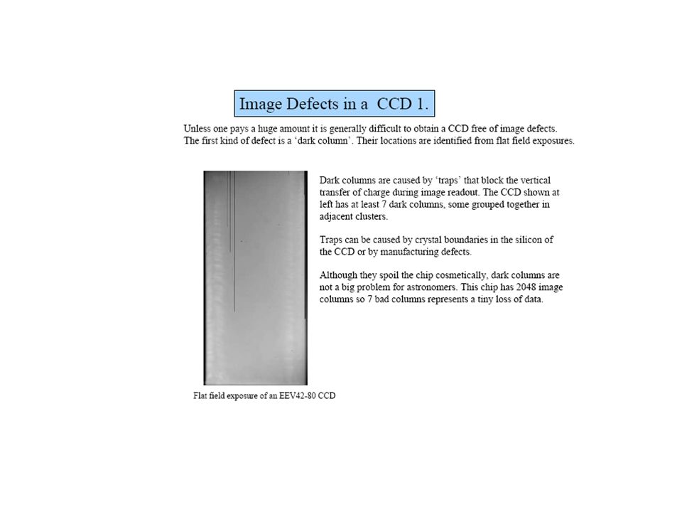
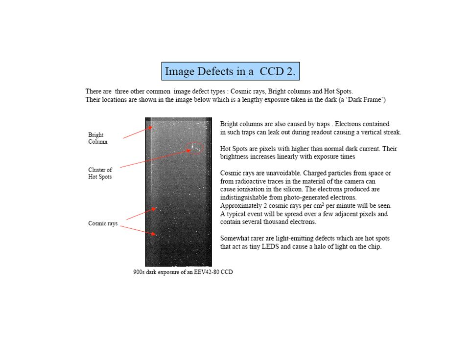
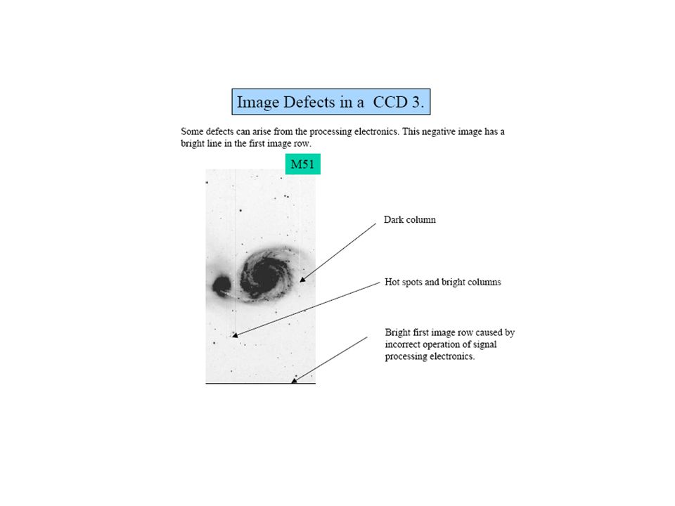
13
CCD 측정 CCD counts : bias + dark current + signal related to the number of electrons liberated by photons in each pixel Only fraction of photons generate electrons ; QE Photons = number of electrons (bias & dark removed) /QE = gain * DN / QE CCD = integrating device is controlled by a mechanical shutter or electrically( changing voltages in CCD) READ NOISE : on-chip amps average noise per pixel = read noise : 5 -20 electrons per pixel per read out (same whether exp 0.1 or 3 hours) Bias frame :simply read out zero image = bias signal changing with changing CCD Temp, also with read noise Dark frame : Without any light, signal caused by thermal excitation of electrons in the CCD : very sensitive to Temp cooling
 /QE = gain * DN / QE CCD = integrating device is controlled by a mechanical shutter or electrically( changing voltages in CCD) READ NOISE : on-chip amps average noise per pixel = read noise : electrons per pixel per read out (same whether exp 0.1 or 3 hours) Bias frame :simply read out zero image = bias signal changing with changing CCD Temp, also with read noise Dark frame : Without any light, signal caused by thermal excitation of electrons in the CCD : very sensitive to Temp cooling")
14
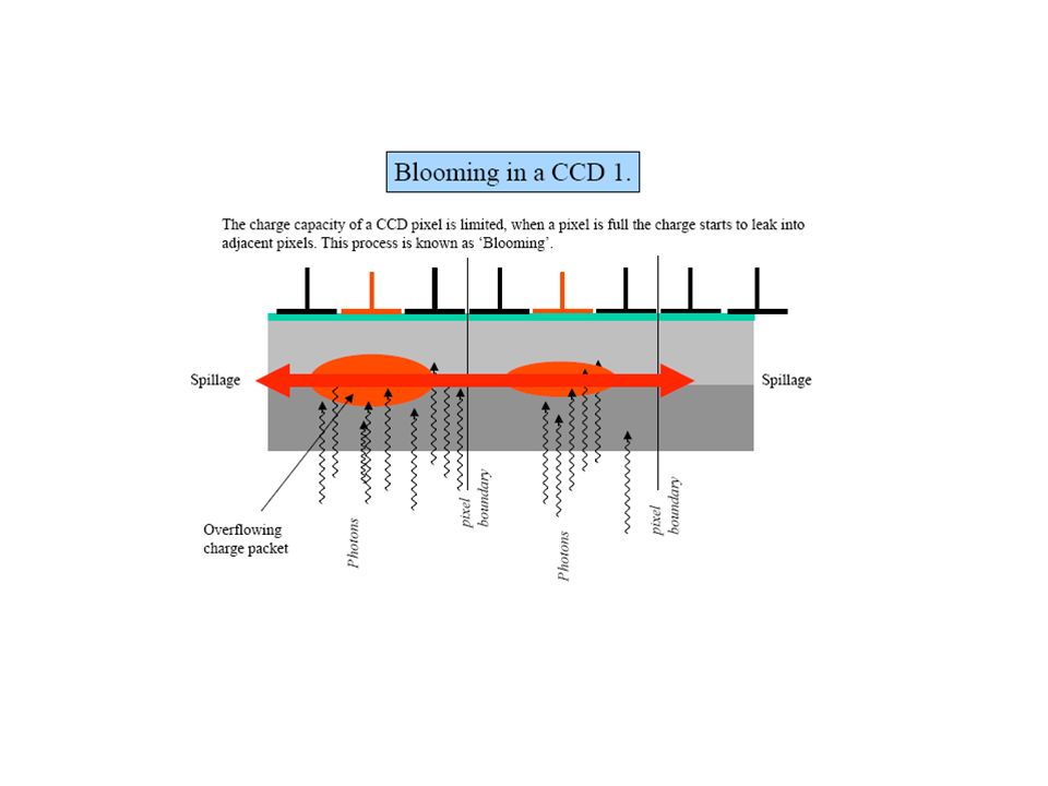
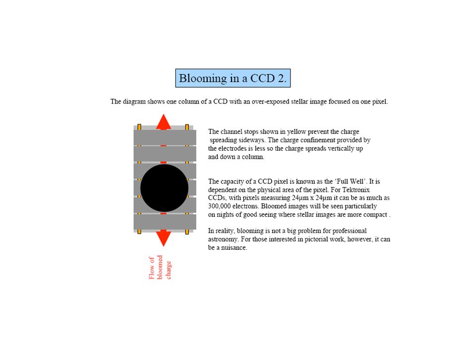
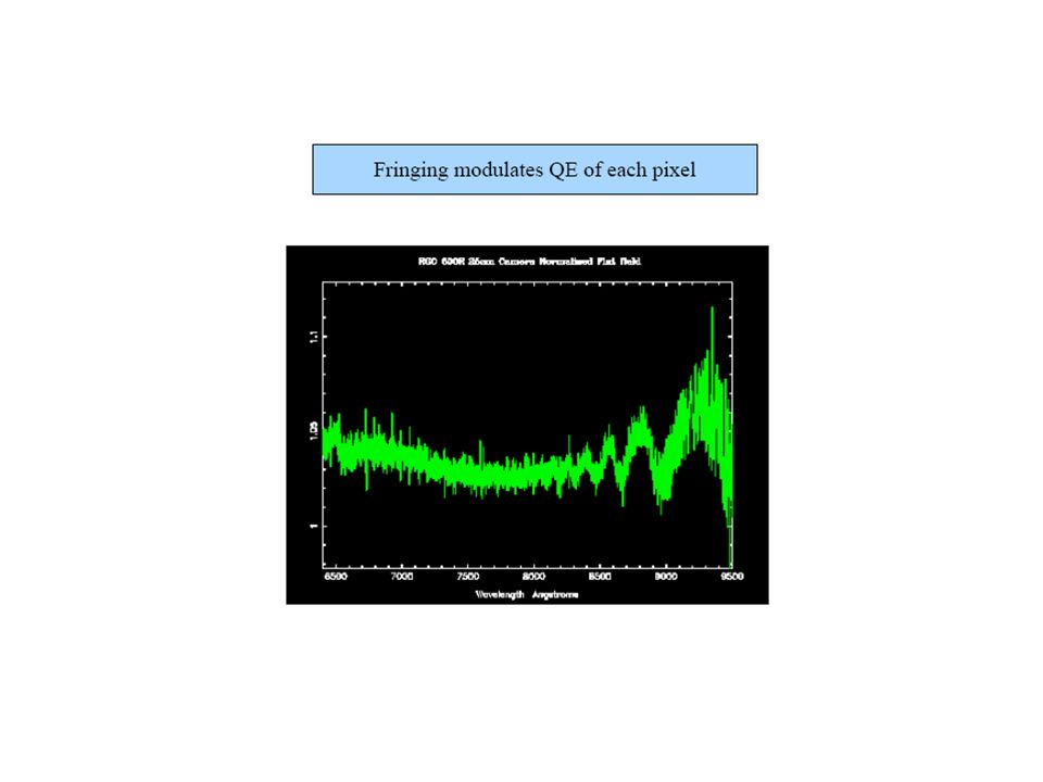
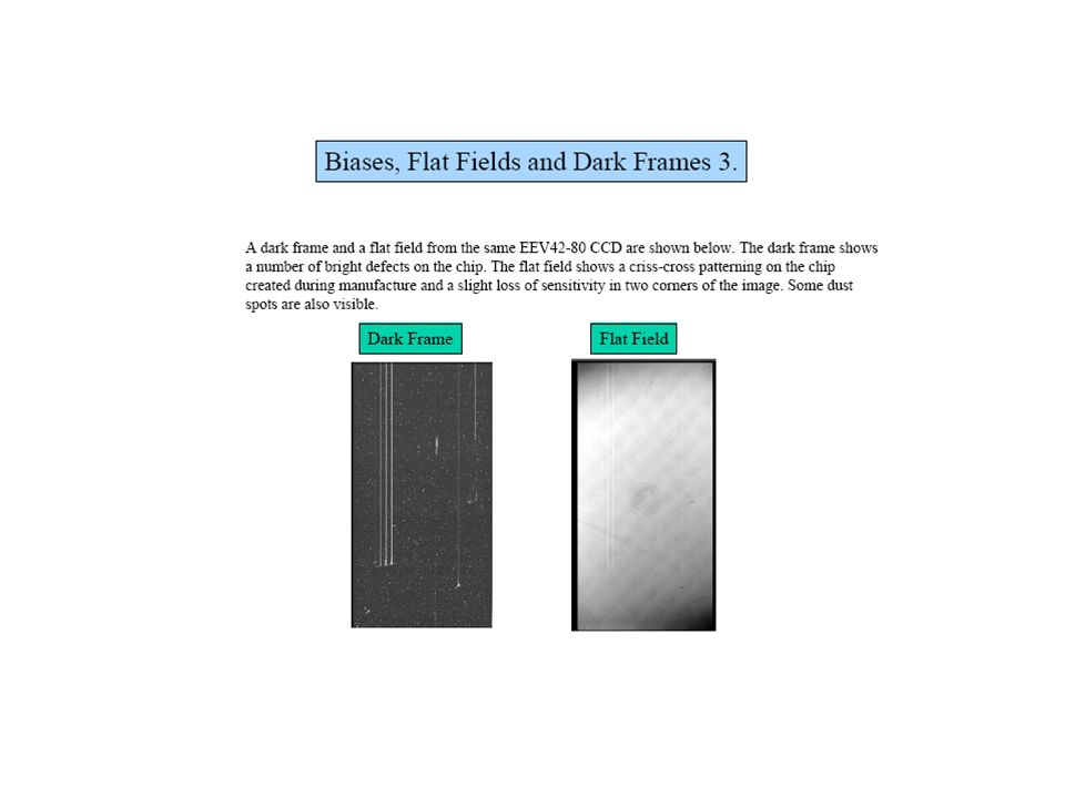
CCD 측정 –cont Flat frame : uniformly illuminating the CCD will NOT generate an equal signal in each pixel ; small scale (pixel to pixel) sensitivity variation : caused by slight differences in pixel sizes Large scale (over large fraction of chip) sensitivity variation : by small variations in the silicon thickness across the chip These can be up to 10% variations over the chip Data frames : Exp time for best S/N Signal =photons “root N” noise ; no way to get rid of this noise : poisson noise Dark noise, read out noise, cosmic ray
 sensitivity variation : caused by slight differences in pixel sizes Large scale (over large fraction of chip) sensitivity variation : by small variations in the silicon thickness across the chip These can be up to 10% variations over the chip Data frames : Exp time for best S/N Signal =photons root N noise ; no way to get rid of this noise : poisson noise Dark noise, read out noise, cosmic ray")
15
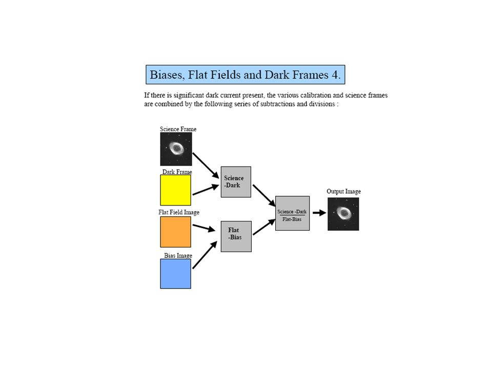
CCD 관측 1. a number of bias frames - median combine to a single low noise bias frame 2. a number of dark frames – no light, finite integration time equal to the data frame integration), combine dark frames into a single low- noise frame (after subtracting bias frames) 3. a number of flat frames in each filter – twilight sky, dome flat (bias, dark subtracted) normalize the flat so that the average signal in each pixel is 1.00 ( simply by dividing by the average signal) 4. subtract low-noise bias frame and low-noise dark frame from object frame. Then, divide this by the normalized frame Reduction frame =[(row-object frame)-(low-noise bias frame)-(low-noise dark frame)]/(normalized flat frame)] Amateur : CCD 20-40 C below the ambient T (0 to -40 C) dark : changes in the dark – source of problems take darks before and after object, these averaged and subtracted from the data frames (here dark really “dark+bias”) inefficient at using telescope time – much used to dark frames
, combine dark frames into a single low- noise frame (after subtracting bias frames) 3. a number of flat frames in each filter – twilight sky, dome flat (bias, dark subtracted) normalize the flat so that the average signal in each pixel is 1.00 ( simply by dividing by the average signal) 4. subtract low-noise bias frame and low-noise dark frame from object frame. Then, divide this by the normalized frame Reduction frame =[(row-object frame)-(low-noise bias frame)-(low-noise dark frame)]/(normalized flat frame)] Amateur : CCD C below the ambient T (0 to -40 C) dark : changes in the dark – source of problems take darks before and after object, these averaged and subtracted from the data frames (here dark really dark+bias ) inefficient at using telescope time – much used to dark frames.")
26
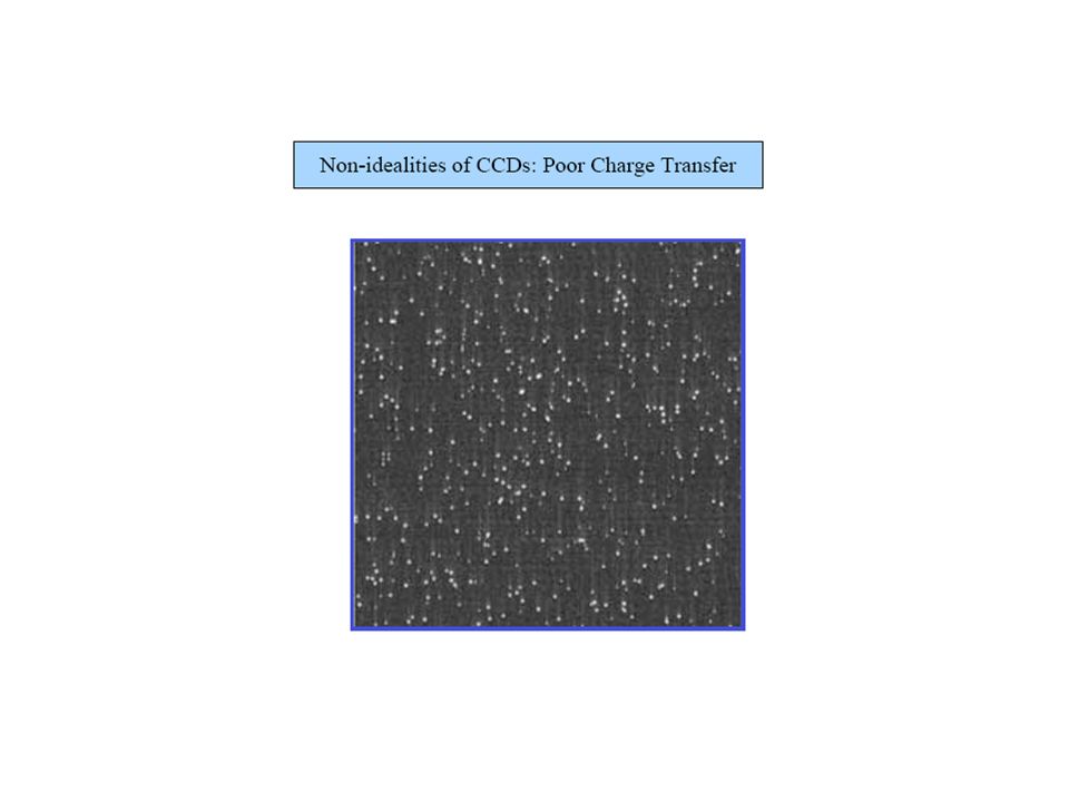
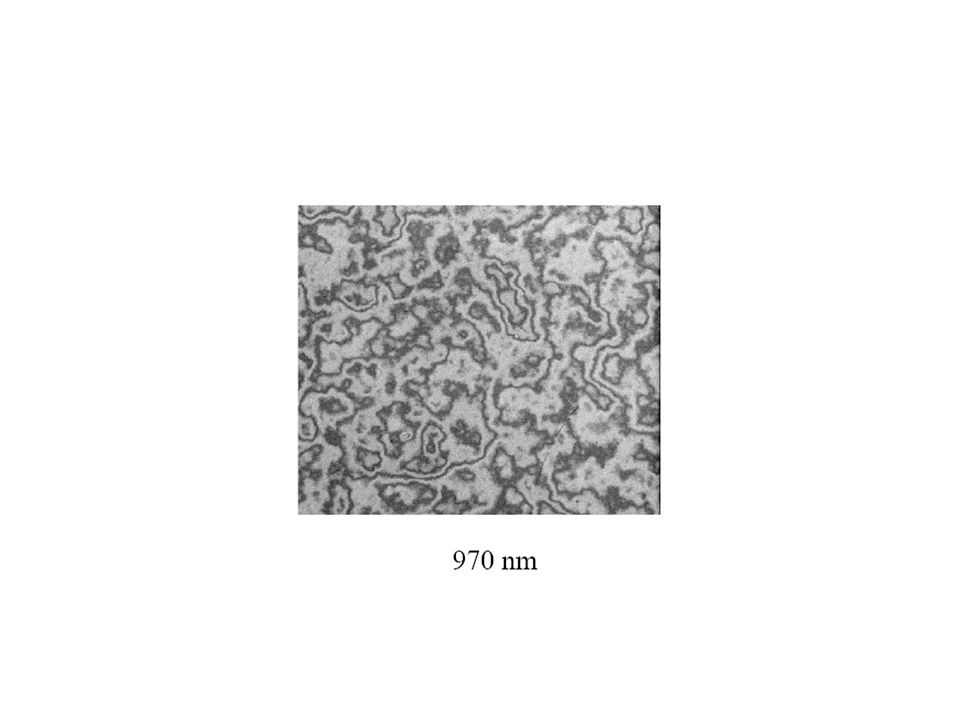
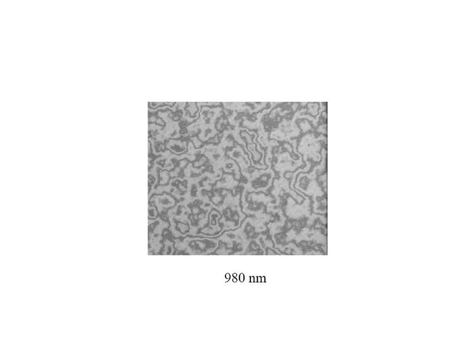
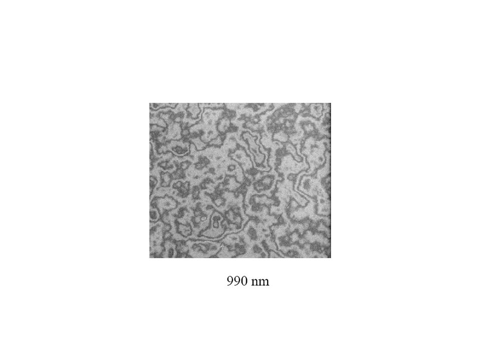
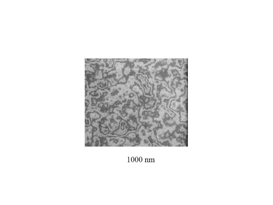
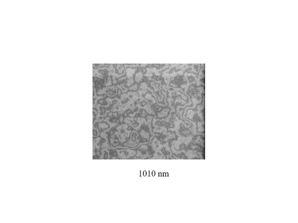
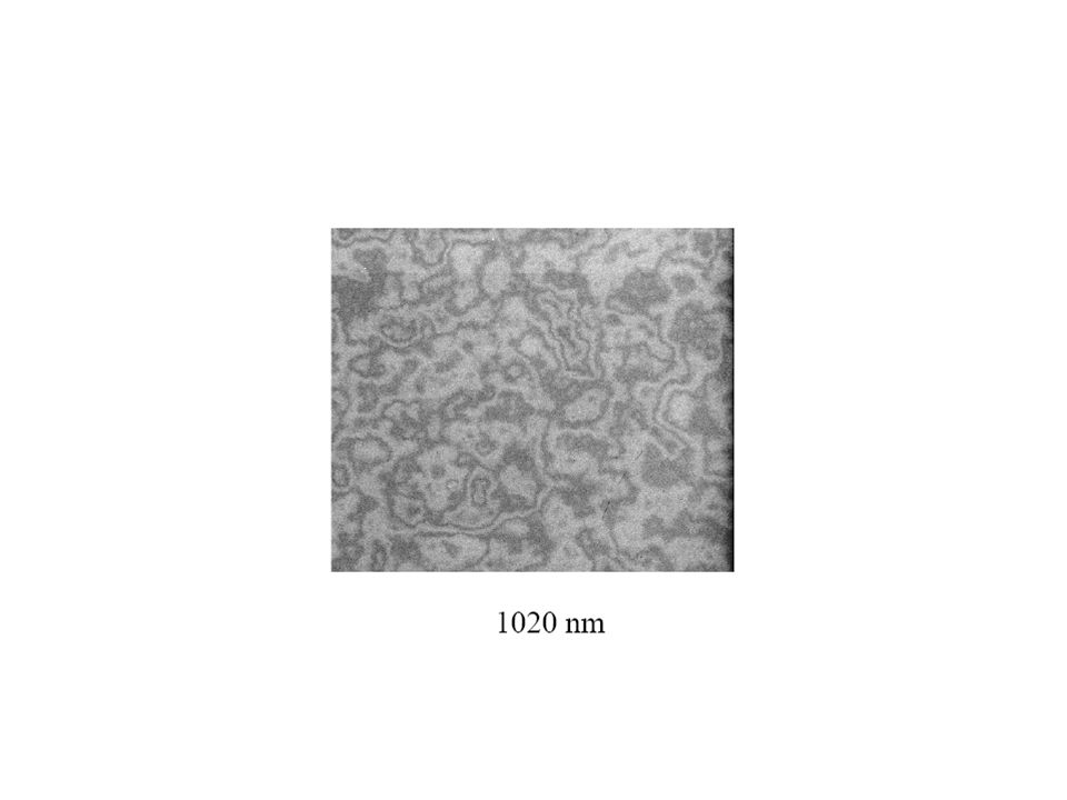
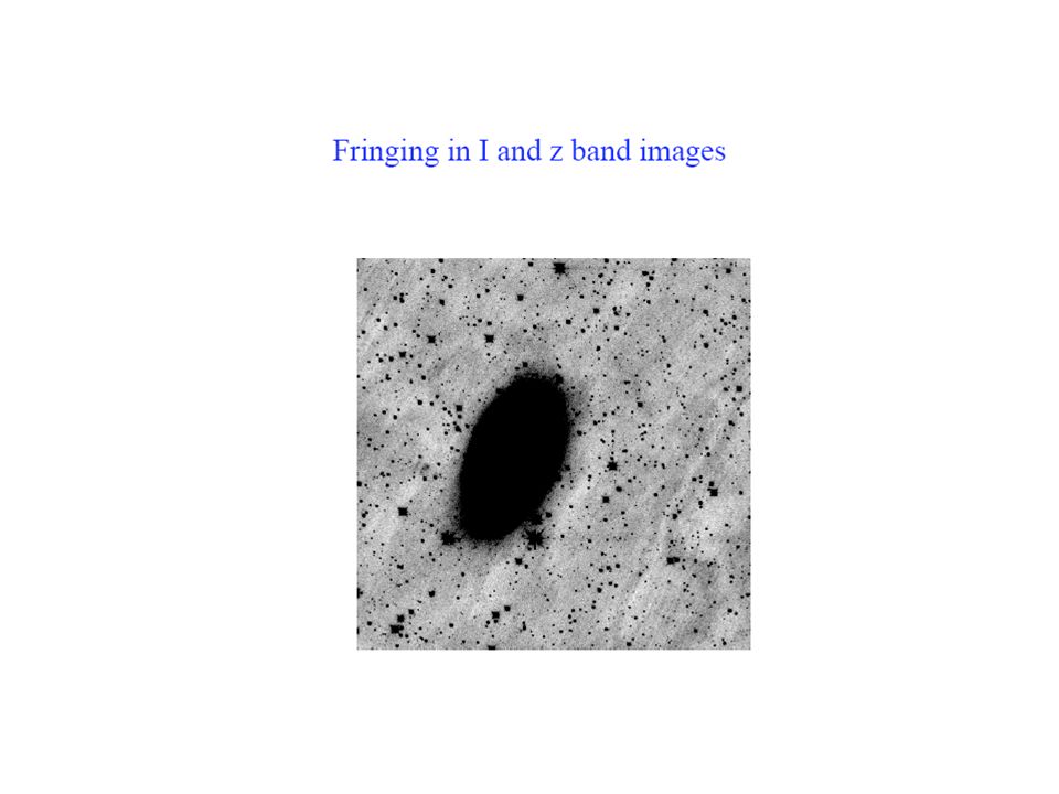
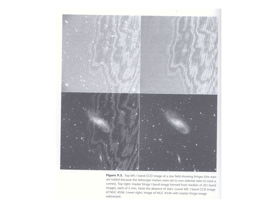
Night sky emission lines produce fringes on a CCD image; also additive noise ; usually in near IR I, Z bands : observe the sparse field with the same exp of the targets

Similar presentations

 - 결과 (outcome) - 사건 (event)>")


 2008.10.28 박사 과정 이종환 011.9640.5025 leejh@astro.snu.ac.kr.>")
.>")


>")