Download presentation
Presentation is loading. Please wait.

1
Chapter 9. 컴퓨터설계기초 9-1 머리말 9-2 데이터 처리장치 (Datapath)
9-1 머리말 9-2 데이터 처리장치 (Datapath) 9-3 산술/논리 연산장치 (ALU) 9-4 Shifter 9-5 Datapath Representation 9-6 Control Word (제어워드) 9-7 Simple Computer Architecture 9-8 Single Cycle Hardwired Control 9-9 Multi Cycle hardwired Control
 9-3 산술/논리 연산장치 (ALU) 9-4 Shifter. 9-5 Datapath Representation. 9-6 Control Word (제어워드) 9-7 Simple Computer Architecture. 9-8 Single Cycle Hardwired Control. 9-9 Multi Cycle hardwired Control.")
2
9-1 머리말 제어장치와 메모리가 결합된 표준 데이터처리장치는 프로그램 가능한 시 스템이며, 이런 것을 단순 컴퓨터라 함
제어장치와 메모리가 결합된 표준 데이터처리장치는 프로그램 가능한 시 스템이며, 이런 것을 단순 컴퓨터라 함 명령어 셋 아키텍쳐(Instruction Set Architecture)는 컴퓨터를 설명하는 수단이며, ISA 를 구현하기 위해서는 제어장치와 데이터 처리장치를 결 합하여 CPU 를 구성한다 단순 컴퓨터에 대한 구조 (Architecture)는 전형적으로 데이터 처리장치 (Datapath) 와 제어장치 (Control Unit) 로 나뉜다 데이터 처리장치의 구성요소 1. 레지스터의 집합 2. 레지스터에 저장된 데이터에 대한 microoperation 3. 제어 인터페이스
는 컴퓨터를 설명하는 수단이며, ISA 를 구현하기 위해서는 제어장치와 데이터 처리장치를 결 합하여 CPU 를 구성한다. 단순 컴퓨터에 대한 구조 (Architecture)는 전형적으로 데이터 처리장치 (Datapath) 와 제어장치 (Control Unit) 로 나뉜다. 데이터 처리장치의 구성요소. 1. 레지스터의 집합. 2. 레지스터에 저장된 데이터에 대한 microoperation. 3. 제어 인터페이스.")
3
9-2 Datapaths ALU (Arithmetic Logic Unit)
/ To perform a microoperation, the contents of specified source registers are applied to the inputs of the shared ALU. Set of register와 ALU 간의 interconnecting path 가 system의 datapath 이다. Datapath는 Register 뿐 아니라 여러 종류의 microoperation을 구현하 는 digital logic을 포함하고 있다. / Digital logic에는 bus, MUX, decoder 그리고 processing unit로 구성

4
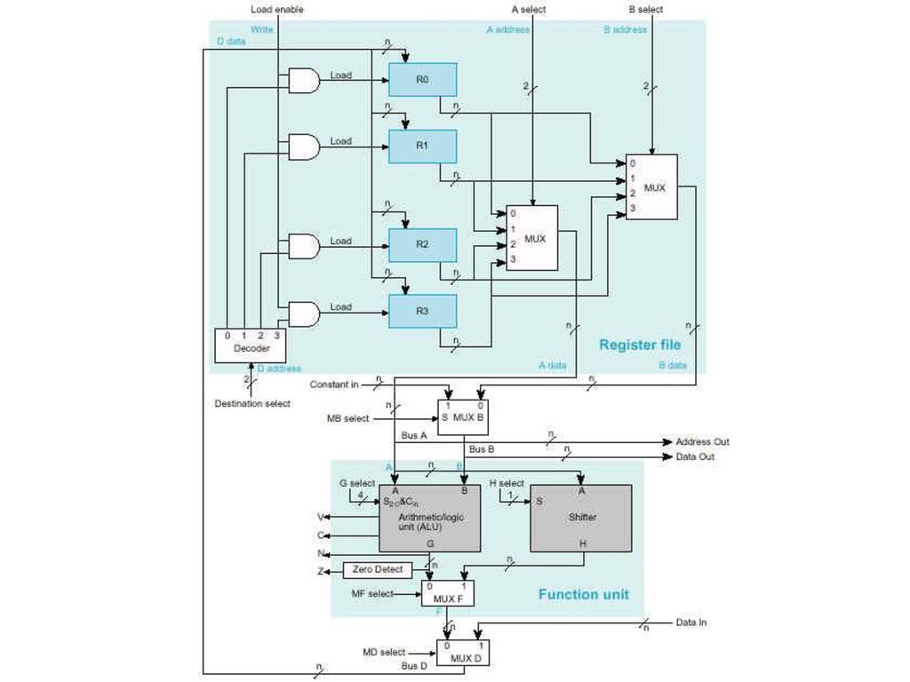
Datapaths 의 Block Diagram [그림 9-1]
![Datapaths 의 Block Diagram [그림 9-1]](http://slidesplayer.org/slide/11328178/61/images/4/Datapaths+%EC%9D%98+Block+Diagram+%5B%EA%B7%B8%EB%A6%BC+9-1%5D.jpg "Datapaths 의 Block Diagram [그림 9-1]")
5
Datapaths 의 Block Diagram [그림 9-1]
Simple bus-based datapath with four registers, an ALU, and a shifter Two MUXes to form ALU input buses A and B Bus B 는 MUX B 에 연결 : 외부 data 받아들임 G select inputs : 어느 microoperation이 수행될 것인가를 결정 H select inputs : select a shift microoperation MUX F selects the output of ALU or the output of the shifter MUX D selects the output of MUX F or external data applied to Data in to be applied to Bus D. Bus D is connected to the inputs of all registers.
![Datapaths 의 Block Diagram [그림 9-1]](http://slidesplayer.org/slide/11328178/61/images/5/Datapaths+%EC%9D%98+Block+Diagram+%5B%EA%B7%B8%EB%A6%BC+9-1%5D.jpg "Simple bus-based datapath with four registers, an ALU, and a shifter. Two MUXes to form ALU input buses A and B. Bus B 는 MUX B 에 연결 : 외부 data 받아들임. G select inputs : 어느 microoperation이 수행될 것인가를 결정. H select inputs : select a shift microoperation. MUX F selects the output of ALU or the output of the shifter. MUX D selects the output of MUX F or external data applied. to Data in to be applied to Bus D. Bus D is connected to the inputs of all registers.")
6
R1 ← R2 + R3 Microoperation을 실행할 경우
Control Unit 는 다음의 control input에 대하여 binary selection 값을 공급해야 한다. 1. A select, to place the contents of R2 onto A data and, hence, Bus A. 2. B select, to place the contents of R3 onto the "0" input of MUX B ; and MB select, to put the "0" input of MUX B onto Bus B. 3. G select, to provide the arithmetic operation A+B. 4. MF select, to place the ALU output on the MUX F output. 5. MD select, to place the MUX F output onto Bus D. 6. Destination select, to select R1 as the destination of the data on Bus D. 7. Load enable, to enable a register 이 경우, R1 이 load 된다.

8
9-3 Arithmetic Logic Unit (산술/논리 연산 장치)
ALU ; 기본적인 산술 및 논리 microoperation을 수행하는 조합논리회로 Selection lines are decoded within the ALU. ; Selection lines are used to determine the operation to be performed. [그림 9-2] n-bit ALU의 기호

9
n-Bit ALU n-bit ALU. A, B ; inputs G ; output
S2 ; Arithmetic or Logic operations 선택 S0 , S1; functions-select inputs to specify the particular arithmetic or logical operation to be performed. 4가지의 Arithmetic and Logical operation 수행 가능 [그림 9-2] n-bit ALU의 기호

10
Arithmetic Circuit (산술 연산회로)
- Basic component is Parallel Adder - Arithmetic sum is calculated as follows G = X + Y + Cin [그림 9-3] 산술 연산회로의 Block diagram

11
Function table for Arithmetic Circuit
S1, S0의 값에 따라 Y input을 control 할 수 있음. Decrement (G=A-1) 의 경우 ; -1 을 2의 보수로 표시하면 “1111” 이 된다.
 의 경우. ; -1 을 2의 보수로 표시하면 1111 이 된다.")
12
B input logic 회로 n 개의 MUX를 이용하여 구현 가능
; Stage i (i=0,1,...n-1)에서의 각 MUX의 입력은 0, Bi, Bi', and 1 이다. 각 입력의 selection input은 S1S0 : 00, 01, 10, 11 이다. ; Arithmetic circuit can be constructed with n full adders and n (4-to-1) MUXs.
에서의 각 MUX의 입력은 0, Bi, Bi , and 1 이다. 각 입력의 selection input은 S1S0 : 00, 01, 10, 11 이다. ; Arithmetic circuit can be constructed with n full adders and n (4-to-1) MUXs.")
13
B input logic 의 설계 S1, S0, Bi are inputs and Yi is output.
Yi = BiS0 + BiS1 S1, S0 are common to all n stage. 각 stage의 i 는 입력 Bi와 출력 Yi와 연관되어있다. (여기서 i = 0,1,2,.....,n 이다) [그림 9-4] 산술 연산회로의 한 단계에 대한 B 입력 논리회로
 [그림 9-4] 산술 연산회로의 한 단계에. 대한 B 입력 논리회로.")
14
Logic diagram of a 4-bit arithmetic circuit
S1, S0, Cin : selection variable S1, S0 는 Fig.7-12(b)의 B.F 식에 따라 Full Adder의 모든 Y 입력을 control 한 다. 8 개의 arithmetic operation은 표7-7 에 list up 되어 있다. ※ Transfer 가 두 개 있음을 유의 [그림 9-5] 4-bit 산술 연산회로의 Logic diagram
의 B.F 식에 따라 Full Adder의 모든 Y 입력을 control 한 다. 8 개의 arithmetic operation은 표7-7 에 list up 되어 있다. ※ Transfer 가 두 개 있음을 유의. [그림 9-5] 4-bit 산술 연산회로의. Logic diagram.")
15
Logic Circuit Design(논리 연산회로)
- One stage of the logic circuit ; Consists of 4 gates(AND, OR, EX-OR, NOT) and 4-to-1 MUX - A typical stage with subscript i. 따라서 n bit를 위한 logic circuit을 구현하려면 [그림 9-6]과 같은 diagram이 n 번 반복되어야 한다. (여기서 i = 0,1,2,.....,n 이다) [그림 9-6] 논리 연산회로의 한 단계
 and 4-to-1 MUX. - A typical stage with subscript i. 따라서 n bit를 위한 logic circuit을 구현하려면 [그림 9-6]과 같은 diagram이 n 번 반복되어야 한다. (여기서 i = 0,1,2,.....,n 이다) [그림 9-6] 논리 연산회로의 한 단계.")
16
Arithmetic/Logic Unit
[그림 9-7] shows just one typical stage of the ALU. 그러므로 n-bit ALU를 구현하려면 위 그림이 n 번 반복되어야 한다. [그림 9-7] ALU 의 한 단계

17
Function Table for ALU [표 9-2] ALU 에 대한 함수표
![Function Table for ALU [표 9-2] ALU 에 대한 함수표](http://slidesplayer.org/slide/11328178/61/images/17/Function+Table+for+ALU+%5B%ED%91%9C+9-2%5D+ALU+%EC%97%90+%EB%8C%80%ED%95%9C+%ED%95%A8%EC%88%98%ED%91%9C.jpg "Function Table for ALU [표 9-2] ALU 에 대한 함수표")
Similar presentations
 명령어 세트 : 특성과 기능 남영진>")


>")

>")


.>")

>")
>")


