Download presentation
Presentation is loading. Please wait.

1
Chapter 5 Etching 5.1 Wet Chemical Etching 5.2 Dry Etching
5.3 Etch Simulation 5.4 Summary

2
PROCESS PARAMETERS Excitation Geometrical Frequency Factors (Surface)
Gas Flow Rate Nature of Surface Excitation Power Potential of Surface Nature of Discharge Gas Temperature of surface Pumping speed Geometrical Factors (Reactor)
")
7
• The pattern transfer is accomplished by an etching process that
that selectively removes unmasked portions of a layer. 5.1 Wet Chemical Etching. • ingot로부터 얇게 베어진 반도체 wafer로부터 출발 할 때 chemical etchants가 lapping과 polishing (optically flat, damage-free surface 하게 하기 위하여)을 위하여 사용된다. • thermal oxidation 혹은 epitaxial growth 하기 전에 contamination을 제거하기 위하여 반도체는 chemically cleaned 하여야 한다. • wet chemical etching은 polysilicon, oxide, nitride, metals, 그리고 Ⅲ-Ⅴ compounds의 blanket etches (i.e., over the whole wafer surface)를 위하여 적당하다.
을 위하여 사용된다. • thermal oxidation 혹은 epitaxial growth 하기 전에 contamination을. 제거하기 위하여 반도체는 chemically cleaned 하여야 한다. • wet chemical etching은 polysilicon, oxide, nitride, metals, 그리고. Ⅲ-Ⅴ compounds의 blanket etches (i.e., over the whole wafer. surface)를 위하여 적당하다.")
8
• wet chemical etching의 mechanisms; three steps.
① reactants가 diffusion에 의하여 reacting 표면으로 운반된다. ② chemical reaction이 표면에서 일어난다. ③ 표면으로부터 생성물이 diffusion 에 의하여 제거된다. ※ etchant solution의 agitation과 temperature가 etch rate에 영향을 끼친다. Figure 5.1 Basic mechanisms in wet chemical etching.

9
5.1.1 Silicon Etching. • etch rate는 uniform하여야 한다.
across a wafer, from wafer to wafer, from run to run, for any variation in feature sizes, pattern densities. 5.1.1 Silicon Etching. Si을 위하여 가장 일반적으로 사용되는 etchants. • nitric acid (HNO3)와 hydrofluoric acid. (HF) • acetic acid. (CH3COOH). • 물은 희석을 위하여 사용. • oxidation reaction; Si + 4HNO3 → SiO2 + 2H2O + 4NO2 (2) • SiO2를 녹이기 reaction; SiO2 + 6HF → H2SiF6 + 2H2O (3)
와 hydrofluoric acid. (HF) • acetic acid. (CH3COOH). • 물은 희석을 위하여 사용. • oxidation reaction; Si + 4HNO3 → SiO2 + 2H2O + 4NO2 (2) • SiO2를 녹이기 reaction; SiO2 + 6HF → H2SiF6 + 2H2O (3)")
10
orientation-dependent etching.
• mixture of KOH in water and isopropyl alcohol. (예) a solution with 19 wt% KOH in deionized (DI) water at about 80℃ 에 대한 etch rate. 0.6 ㎛/min for the (100) – plane. 0.1 ㎛/min for the (110) – plane. 0.006 ㎛/min (60Å/min) for the (111)-plane. etch rate의 비 (100) : (110) : (111) = 100 : 16 : 1
 a solution with 19 wt% KOH in deionized (DI) water at about 80℃ 에 대한 etch rate. 0.6 ㎛/min for the (100) – plane. 0.1 ㎛/min for the (110) – plane ㎛/min (60Å/min) for the (111)-plane. etch rate의 비 (100) : (110) : (111) = 100 : 16 : 1.")
11
Figure 5.2 Orientation-dependent etching. (a) Through window patterns on <100>-oriented silicon. (b) Through window patterns on <110>-oriented silicon.
 Through window patterns on <110>-oriented silicon.")
12
5.1.2 Silicon Dioxide Etching.
• a dilute solution of HF with or without the addition of ammonium fluoride (NH4F) • buffered HF solution. (BHF). buffered oxide etch. (BOE). PH value를 조절 → stable etching performance를 유지한다. • SiO2의 etch rate; etchant solution, etchant concentration agitation, temperature에 의존. • oxide에 있어서 density, porosity, microstructure, impurities의 존재 등이 etch rate에 영향을 끼친다. (예). Oxide에 고농도의 phosphorus가 있으면 rapid. CVD에 의하여 형성된 loosely structured oxide는 열적으로 grown oxide 보다 faster etch rate. HF + NH4F.
 • buffered HF solution. (BHF). buffered oxide etch. (BOE). PH value를 조절 → stable etching performance를 유지한다. • SiO2의 etch rate; etchant solution, etchant concentration agitation, temperature에 의존. • oxide에 있어서 density, porosity, microstructure, impurities의 존재 등이. etch rate에 영향을 끼친다. (예). Oxide에 고농도의 phosphorus가 있으면 rapid. CVD에 의하여 형성된 loosely structured oxide는 열적으로. grown oxide 보다 faster etch rate. HF + NH4F.")
13
5.1.3 Silicon Nitride and Polysilicon Etching.
Si3N4 • concentrated HF. 혹은 buffered HF. at room temperature. • boiling H3PO4. selective etching of nitride to oxide; 85% H3PO4 at 180℃ (이 solution이 SiO2는 대단히 천천히 공격한다.) • etch rate; 10nm/min for Si3N4. (1nm/min for SiO2). • boiling H3PO4 solution으로써 nitride를 etching할 때 P.R의 adhesion 문제가 있다. • Better patterning; P.R/SiO2/Si3N4. resist pattern을 oxide layer로 transfer. oxide layer는 nitride etching을 위한 masks로서 작용. polysilicon etching; single-crystal silicon etching과 비슷. 그러나 etch rate는 grain boundaries 때문에 훨씬 빠르다. dopant농도, 온도가 etch rate에 영향을 끼친다.
 • etch rate; 10nm/min for Si3N4. (1nm/min for SiO2). • boiling H3PO4 solution으로써 nitride를 etching할 때 P.R의 adhesion. 문제가 있다. • Better patterning; P.R/SiO2/Si3N4. resist pattern을 oxide layer로 transfer. oxide layer는 nitride etching을 위한 masks로서 작용. polysilicon etching; single-crystal silicon etching과 비슷. 그러나 etch rate는 grain boundaries 때문에 훨씬 빠르다. dopant농도, 온도가 etch rate에 영향을 끼친다.")
14
5.1.5 Gallium Arsenide Etching.
5.1.4 Aluminum Etching 73% H3PO4, 4% HNO3, 3.5% CH3COOH 19.5% DI water at 30℃ to 80℃ • HNO3가 Al을 산화시키고, H3PO4는 산화된 aluminum을 녹인다. • etchant 농도, 온도, agitation, impurities에 etch rate가 의존한다. • copper가 Al에 첨가 되었을 때 etch rate는 낮아진다. 5.1.5 Gallium Arsenide Etching. H2SO4-H2O2-H2O and H3PO4-H2O2-H2O Systems. H2SO4 : H2O2 : H2O = 8 : 1 : 1 (volume ratio). 0.8㎛/min for the <111> Ga face. 1.5㎛/min for all other faces. = 3 : 1 : 50 (volume ratio). 0.4㎛/min for the <111> Ga face. 0.8㎛/min for all other faces.
. 0.8㎛/min for the <111> Ga face. 1.5㎛/min for all other faces. = 3 : 1 : 50 (volume ratio). 0.4㎛/min for the <111> Ga face. 0.8㎛/min for all other faces.")
16
5.2 Dry Etching. Figure 5.3 Comparison of wet chemical etching
and dry etching for pattern transfer.

17
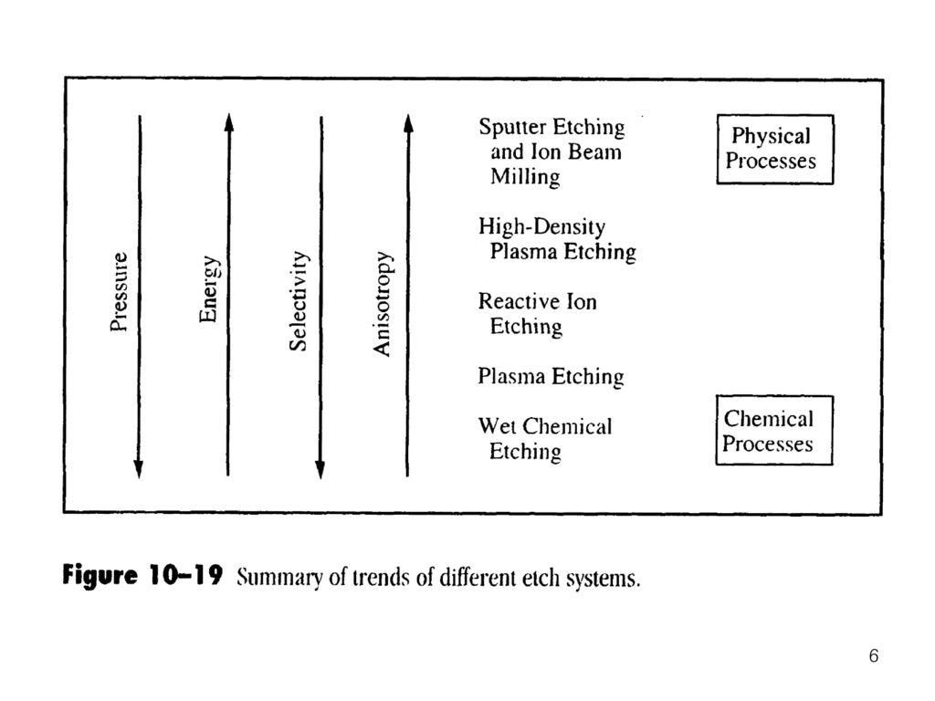
• wet chemical etching; isotropic ( the lateral and vertical etch rates are the
same; Fig5.3.b) • anisotropic etching ; Fig 5.3.c • Dry etching; plasma-assisted etching, plasma etching, reactive ion etching (RIE), sputter etching, magnetically enhanced RIE (MERIE), reactive ion beam etching, high-density plasma (HDP) etching. ※ isotropic etching; wet chemical etching의 주요 단점; undercutting.
 • anisotropic etching ; Fig 5.3.c. • Dry etching; plasma-assisted etching, plasma etching, reactive ion etching (RIE), sputter etching, magnetically enhanced RIE (MERIE), reactive ion beam etching, high-density plasma (HDP) etching. ※ isotropic etching; wet chemical etching의 주요 단점; undercutting.")
18
5.2.1 Plasma Fundamentals. A plasma is a fully or partially ionized gas composed of equal numbers of positive and negative charges and a different number of unionized molecules. plasma의 발생. • 충분히 큰 electric field가 gas에 인가된다. • gas가 breakdown되어 ion화 된다. • plasma는 free electron (어떤 수단에 즉, 음으로 biased된 전극으로 부터 field emission에 의하여 released 된)에 의하여 시작된다. • free electron은 전기장으로부터 kinetic energy를 얻고 가속된다. • electron은 gas molecules와 충돌하여 energy를 잃고 gas molecules는 ion화 한다. (free electron이 생김). • applied voltage가 breakdown potential 보다 크면 plasma는 계속 유지 된다.
에 의하여 시작된다. • free electron은 전기장으로부터 kinetic energy를 얻고 가속된다. • electron은 gas molecules와 충돌하여 energy를 잃고 gas molecules는. ion화 한다. (free electron이 생김). • applied voltage가 breakdown potential 보다 크면 plasma는 계속 유지. 된다.")
19
• dry etching을 위한 plasma에서 electron의 concentration은 전형적으로
109 ~ 1012 cm-3 . • 1 torr 압력에서 gas molecules의 농도는 electron농도보다 104 ~107배 더 높다. 이것은 50℃ ~100℃ 범위의 평균 gas temperature가 되게 한다. 그러므로 plasma-assisted dry etching은 low-temperature process이다. ※ 전자 온도 (electron temperature); 자유전자를 포함하는 계에서 자유 전자의 energy분포에 대응하는 온도를 말한다. (온도의 등가전압; volt-equivalent of temperature) ; Einstein relationship. ※ room temperature에서 VT=0.0259V.
; 자유전자를 포함하는 계에서 자유. 전자의 energy분포에 대응하는 온도를 말한다. (온도의 등가전압; volt-equivalent of temperature) ; Einstein relationship. ※ room temperature에서 VT=0.0259V.")
20
5.2.2 Etch Mechanism, Plasma Diagnostics, and End-Point control.
• plasma etching proceeds in five steps. ① etchant species 발생. ② stagnant gas layer를 통하여 표면으로 확산. ③ 표면에 흡수. ④ chemical reaction. ⑤ volatile compounds가desorbed. 그리고 diffusion. Figure Basic steps in a dry etching process.

21
physical methods and chemical methods.
• physical etching ( sputter etching이 포함 된다). positive ions이 high speed로 표면을 bombard한다. anisotropic profiles, low etch selectivity, high bombardment-induced damage. • chemical etching. plasma에 의하여 발생된 neutral reactive species가 material surface와 작용하여 volatile products를 형성한다. high etch rate, good selectivity, isotropic profile. • combinations of chemical and physical etching (예; RIE). anisotropic etch profile, reasonably good selectivity, moderate bombardment-induced damage.
. positive ions이 high speed로 표면을 bombard한다. anisotropic profiles, low etch selectivity, high bombardment-induced damage. • chemical etching. plasma에 의하여 발생된 neutral reactive species가 material surface와. 작용하여 volatile products를 형성한다. high etch rate, good selectivity, isotropic profile. • combinations of chemical and physical etching (예; RIE). anisotropic etch profile, reasonably good selectivity, moderate bombardment-induced damage.")
22
Plasma Diagnostics. End-Point Control.
• Most processing plasmas emit radiation in the range from infrared to ultraviolet. • OES ( optical emission spectroscopy). 관찰된 spectral peak를 사용하여, 이전에 결정된 spectral series와 이들 emission의 상관관계에 의하여 neutral과 ionic species의 존재를 결정한다. End-Point Control. • Dry etching은 underlying layer에 대하여 etch 선택성이 나쁘므로, etching process가 종결되어 질 때를 나타내는 monitor (i.e. , an end-point detection system)가 있어야 한다. • Laser interferometry.
. 관찰된 spectral peak를 사용하여, 이전에 결정된 spectral series와 이들. emission의 상관관계에 의하여 neutral과 ionic species의 존재를 결정한다. End-Point Control. • Dry etching은 underlying layer에 대하여 etch 선택성이 나쁘므로, etching. process가 종결되어 질 때를 나타내는 monitor (i.e. , an end-point detection. system)가 있어야 한다. • Laser interferometry.")
23
Figure 5.5 (p. 93) The relative reflectance of the etching surface of a composite silicide/poly-Si layer. The end point of the etch is indicated by the cessation of the reflectance oscillation.

24
5.2.3 Reactive Plasma Etching Techniques and Equipment.
• plasma processing의 first application; photoresist stripping.

25
Figure 5.6 Comparison of ion energy and operating pressure ranges for different types of plasma reactors.

26
Reactive Ion Etching. • In a parallel-plate diode system, a radio frequency capacitively coupled bottom electrode holds the wafer. • grounded electrode의 큰 면적, lower operating pressure (<500 mTorr).가 wafer surface에서 큰 negative self-bias가 되게 하여 plasma로 부터 energetic ions의 wafer에 heavy bombardment한다. • etch selectivity가 비교적 낮다. (적당한 etch chemistry를 선택하여 개선할 수 있다).
.가. wafer surface에서 큰 negative self-bias가 되게 하여 plasma로 부터. energetic ions의 wafer에 heavy bombardment한다. • etch selectivity가 비교적 낮다. (적당한 etch chemistry를 선택하여 개선할 수 있다).")
27
Figure 5.7 Schematic of a triode reactive ion etch reactor. The ion energy is separately controlled by a bias voltage on the bottom electrode. rf, radio frequency. • triode-configuration RIE etch. • separate bias를 통하여 wafer electrode 위의 ion energy를 control 할 수 있다. 따라서 선택성의 손실과 ion bombardment-induced damage를 최소화 할 수 있다.

28
Electron Cyclotron Resonance Plasma Etching.
• most parallel-plate plasma etcher들은 plasma parameters (electron energy, plasma density, reactant density 등 )을 독립적으로 control 할 수 없다. 따라서 ion bombardment-induced damage가 매우 심각하다. • electron cyclotron resonance (ECR) reactor는 microwave power를 static magnetic field와 결합 (combine)했다. electron들이 magnetic field lines 주위를 angular frequency에서 돈다. 이 frequency가 applied microwave frequency와 같을 때 공진이 일어나고 그 결과 a high degree of dissociation and ionization (10-2 for ECR compared with for RIE)이 일어난다. • ECR plasma system은 thin film deposition을 위하여도 사용된다. ( thermal activation 없이 room temperature에서 가능).
을 독립적으로 control. 할 수 없다. 따라서 ion bombardment-induced damage가 매우 심각하다. • electron cyclotron resonance (ECR) reactor는 microwave power를. static magnetic field와 결합 (combine)했다. electron들이 magnetic field lines 주위를 angular frequency에서 돈다. 이 frequency가 applied microwave frequency와 같을 때 공진이 일어나고. 그 결과 a high degree of dissociation and ionization (10-2 for ECR. compared with 10-6 for RIE)이 일어난다. • ECR plasma system은 thin film deposition을 위하여도 사용된다. ( thermal activation 없이 room temperature에서 가능).")
29
Figure 5.8 Schematic of an electron cyclotron resonance reactor

30
Other high-Density Plasma Etchers.
high plasma density (1011 ~ 1012 cm-3) and low processing pressure (< 20 m Torr). • inductively coupled plasma (ICP) source. • transformer coupled plasma (TCP) source. • surface wave-coupled plasma (SWP) source. HDP의 장점. better critical dimension (CD) control, high etching rates, better selectivity, low substrate damage ( independent biasing of the substrate and the side electrode potentials) high anisotropy (low pressure, high active species density 때문에). HDP의 단점 complexity, higher cost. Figure Schematic of a transformer-coupled plasma reactor.
 and low processing pressure. (< 20 m Torr). • inductively coupled plasma (ICP) source. • transformer coupled plasma (TCP) source. • surface wave-coupled plasma (SWP) source. HDP의 장점. better critical dimension (CD) control, high etching rates, better selectivity, low substrate damage ( independent. biasing of the substrate and the side. electrode potentials) high anisotropy. (low pressure, high active species density 때문에). HDP의 단점. complexity, higher cost. Figure 5.9 Schematic of a transformer-coupled plasma reactor.")
31
Cluster Plasma Processing.
• 반도체 wafer는 주위 먼지가 많은 오염에 노출을 최소화 하기위하여 clean room에서 공정이 되어야 한다. • 입자 오염을 최소화 하기 위하여 clustered plasma tools가 wafer를 one process chamber에서 다른 곳으로 진공 분위기에서 통과 시키 위하여 wafer handler를 사용한다. Figure (p. 97) Cluster reactive ion etch tool for multilayer metal (TiW/AlCu/TiW) interconnect etching.
 Cluster reactive ion etch tool for multilayer. metal (TiW/AlCu/TiW) interconnect etching.")
32
5.2.4 Reactive Plasma Etching Applications.
• Table 5.3 Etch Chemistries of Different Etch Processes. • etch process를 개발하는 것은 etch rate, selectivity, profile control, critical dimension, damage를 optimizing하는 것을 의미한다. Silicon Trench Etching. • Deep trenches; 5㎛ 이상 깊이, storage capacitor를 형성하기 위하여. shallow trenches; 1㎛ 이하 깊이, isolation을 위하여. • HBr + NF3 + SF6 + O2; trench capacitor를 형성하기 위하여 약 7㎛정도 까지. Figure Dependence of average silicon trench etch rate on aspect ratio.

33
Polysilicon and Polycide Gate Etching.
• polysilicon 혹은 polycide가 MOS devices를 위하여 gate물질로서 사용된다. • anisotropic etching과 high etch selectivity가 gate etching을 위하여 요구되는 중요한 사항이다. • high selectivity 와 etch anisotropy를 동시에 얻기가 어렵다. 그러므로 multistep processing이 사용된다. • chlorine-based 와 bromine-based chemistries가 gate etching을 위하여 사용된다. (etch anisotropy와 selectivity를 얻기 위하여).
.")
34
Dielectric Etching. • dielectrics (특히 SiO2 그리고 Si3N4)의 patterning이 modern semiconductor devices 제조에 있어서 key process이다. • vertical profiles가 sidewall passivation에 의하여 얻어진다. [ carbon-containing fluorine species (예. CF4, CHF3, C4F8)를 plasma에 넣음으로서] • high ion bombardment energies가 oxide로 부터 polymer를 제거하기 위하여 요구된다. • high F concentration이 silicon에서 selectivity를 나쁘게 한다. 따라서 high C/F ratio (예 C2F6, C4F8, C5F8)의 gas를 사용한다.
를 plasma에. 넣음으로서] • high ion bombardment energies가 oxide로 부터 polymer를 제거하기 위하여. 요구된다. • high F concentration이 silicon에서 selectivity를 나쁘게 한다. 따라서 high C/F ratio (예 C2F6, C4F8, C5F8)의 gas를 사용한다.")
35
Interconnect Metal Etching.
• interconnection을 위하여 사용되는 물질; Al, Cu, W. • anisotropic etching이 요구된다. Aluminum etching 동안에 anisotropic etching을 얻기 위하여 carbon-containing gas (예 CHF3) 혹은 N2가 보태어 진다. (sidewall passivation을 형성하기 위하여). • residual chlorine이 atmospheric water와 반응하여 Al을 부식시키는 HCl을 형성한다. • Cl대신 F로 바꾸기 위하여 CF4 discharge에 wafer를 노출시키고, oxygen discharge로써 resist를 제거하고 곧 바로 DI wafer에 담근다. (Al의 부식을 막는다.). • copper; Al보다 low resistivity ( ~ 1.7Ω.cm). electromigration에 대한 우수한 저항성이 있다. 그러나 room temperature에서 plasma etching이 어렵다. • damascene process. • chemical mechanical polishing (CMP).
 혹은 N2가 보태어. 진다. (sidewall passivation을 형성하기 위하여). • residual chlorine이 atmospheric water와 반응하여 Al을 부식시키는 HCl을. 형성한다. • Cl대신 F로 바꾸기 위하여 CF4 discharge에 wafer를 노출시키고, oxygen. discharge로써 resist를 제거하고 곧 바로 DI wafer에 담근다. (Al의 부식을 막는다.). • copper; Al보다 low resistivity ( ~ 1.7Ω.cm). electromigration에 대한 우수한 저항성이 있다. 그러나 room temperature에서 plasma etching이 어렵다. • damascene process. • chemical mechanical polishing (CMP).")
36
• LPCVD tungsten이 contact holes을 채우 는데 사용된다.
; excellent deposition conformability 때문에 Figure Formation of tungsten plug in a contact hole by depositing blanket low-pressure chemical vapor deposition W and then using reaction ion etching etchback. Figure 5.13 Process sequence for the dual damascene process.

37
※ Self-Bias of RF electrodes
• 전계에 의하여 받는 힘 참고자료 : Glow Discharge Processes. (sputtering and plasma etching) John wiley & Sons Brian Chapman (143~146쪽) • charge가 가벼울수록 주어진 field에 대하여 more current 혹은 주어진 전류를 흐르게 하는데 보다 작은 field가 요구된다. • Biased probe immersed in a plasma can draw a large electron current but only a very much smaller ion current because of the much lower mean speed of the ions. Figure 5-4 Schematic of a high frequency glow discharge circuit c : blocking capacitor Va : 교류
 John wiley & Sons Brian Chapman (143~146쪽) • charge가 가벼울수록 주어진 field에. 대하여 more current 혹은 주어진 전류를. 흐르게 하는데 보다 작은 field가 요구된다. • Biased probe immersed in a plasma. can draw a large electron current but only. a very much smaller ion current because of. the much lower mean speed of the ions. Figure 5-4 Schematic of a high frequency. glow discharge circuit. c : blocking capacitor. Va : 교류.")
38
figure 5-5 Voltage and target current waveforms when the circuit of Figure 5-4 is square wave excited

39
• peak-to-peak amplitude of 2kV.
• capacitor가 초기에는 uncharged. • t=0에서 Va가 -1kV. · Vb도 같은 값이 된다. • discharge가 일어나기 시작하며 target이 positive ion에 의하여 bombardment 당한다. • capacitor가 positively charge 되어 target potential Vb가 zero를 향하여 올라간다. • 만약 공급 주파수가 충분히 높다면(~1MHz) Vb는 half crystal 의 끝부분에서 많이 변화하기 않을 것이며, 대략 -800V로 올라갈 것이 추정된다. • 이 순간 Va가 2kV에 의하여 증가된다면, 이 경우 Vb는 +1200V가 될 것이다. • positively charged target는 large electron current를 끌어당긴다. 그리하여 Vb는 ion bombardment일 때 보다 훨씬 빠르게 zero를 향하여 줄어든다. 이것은 비슷한 potential 차이에서 electron current가 ion current보다 훨씬 크다는 본보기 이다. • first cycle 의 끝에서 Vb가 +100V에 도달하는 가정을 한다. 그 때 Va가 switch 되면, Vb는 -1900V로 drop되고, 다시 증가하게 된다. 그러나 ion current는 작으므로, 다시 +2kV 에 의하여 switching 되기 전에 Vb는 그렇게 많이 증가하지 않는다.
 Vb는 half crystal 의 끝부분에서. 많이 변화하기 않을 것이며, 대략 -800V로 올라갈 것이 추정된다. • 이 순간 Va가 2kV에 의하여 증가된다면, 이 경우 Vb는 +1200V가 될 것이다. • positively charged target는 large electron current를 끌어당긴다. 그리하여. Vb는 ion bombardment일 때 보다 훨씬 빠르게 zero를 향하여 줄어든다. 이것은. 비슷한 potential 차이에서 electron current가 ion current보다 훨씬 크다는 본보기. 이다. • first cycle 의 끝에서 Vb가 +100V에 도달하는 가정을 한다. 그 때 Va가 switch 되면, Vb는 -1900V로 drop되고, 다시 증가하게 된다. 그러나. ion current는 작으므로, 다시 +2kV 에 의하여 switching 되기 전에 Vb는 그렇게 많이. 증가하지 않는다.")
40
• 몇 cycle 이후에 voltage wave form은 같은 모양으로 반복하게 된다.
• negative 쪽으로 옮겨지고 target는 high energy ion bombardment 그리고 low energy electron bombardment 하게 된다. • Total charge flow per cycle sums to zero. So that the areas under the electron and ion portions of the current-time wave form must be equal. • target는 self bias 된다.

41
· Vb는 each cycle의 대단히 짧은 부분만 positive가 되므로 target의
Va (kV) t Vb (kV) t DC Offset Figure 5-6 Voltage waveform at generator (Va) and target (Vb) in a conventional sinu- soidally-excited if discharge · dc offset voltage · Vb는 each cycle의 대단히 짧은 부분만 positive가 되므로 target의 ion bombardment는 거의 연속이다.
 t. Vb. (kV) t. DC Offset. Figure 5-6 Voltage waveform at generator (Va) and target (Vb) in a conventional sinu- soidally-excited if discharge. · dc offset voltage. · Vb는 each cycle의 대단히 짧은 부분만 positive가 되므로 target의. ion bombardment는 거의 연속이다.")
Similar presentations


![Chapter 12 Spectroscopy 1 : Rotational & Vibrational Spectra. -- Vacuum wavelength [ cm ] -- Vacuum wavenumber [ cm -1 ]](/39/10994127/big_thumb.jpg "Chapter 12 Spectroscopy 1 : Rotational & Vibrational Spectra. -- Vacuum wavelength [ cm ] -- Vacuum wavenumber [ cm -1 ]>")


. Carbon nanotube( 탄소 나노튜브 ) Multi-walled carbon nanotube.>")

 2008.01.08 Joo Suk-bae. 회절 (Diffraction) 입자의 진행경로에 틈이 있는 장애물이 있으면 입자는 그 틈을 지나 직선으로 진행한다. 이와 달 리 파동의 경우, 틈을 지나는 직선 경로뿐 아니라 그 주변의.>")
 1.CVD(Chemical Vapor Deposition), 화학기상증착 기술이란 ? 먼저 CVD 기술을 이해하기 전에 CVD 기술이 반도체 제조공정 중 어디에 위치하고 어떻게 사용되는지를.>")
 제조공정 Ⅱ -4. MODULE 제조공정 Ⅲ. 단위공정 설명 Ⅲ -1. 증착공정 Ⅲ -2. PHOTO.>")


의 기술이해>")
