Download presentation
Presentation is loading. Please wait.

1
검출기 눈, 사진, Photoelectric device, Photomultipliers, Image intensifiers, Charged Coupled Device,

2
눈 Parnoramc views – large solid angle ( ~ 180 도)
Sub-sec time resolution Enormous range : full sun light – dark night (1010 – 1) But unable to make quantitative measurements, not able to integrate, Not a permanent record 동공 : 최대 8mm 이론적 resolution 16 arcsec (1.22*6000*206265/8* = 16”) cone cells resolution : 1’ 초점거리 :~ 25 mm (조리개 조절) Bright light : photopic (daylight vision by cones) Low light : “dark adapted” or scotopic Night time vision by rods Both == mesopic vision Surface of retina : rods & cones cell Rods more sensitive to faint light than cones Cones only produce sensation of color (3 type)
 But unable to make quantitative measurements, not able to integrate, Not a permanent record. 동공 : 최대 8mm 이론적 resolution 16 arcsec (1.22*6000*206265/8* = 16 ) cone cells resolution : 1’ 초점거리 :~ 25 mm (조리개 조절) Bright light : photopic (daylight vision by cones) Low light : dark adapted or scotopic. Night time vision by rods. Both == mesopic vision. Surface of retina : rods & cones cell. Rods more sensitive to faint light than cones. Cones only produce sensation of color (3 type)")
3
사진 1840 : J.W. Draper record the image of Moon with the newly invented daguerreotype (은판사진-불란서인 Louis Daguerre)process 1870s ; dry emulsion (감광유제):silver bromide crystals in a transparent gelatin Objective in data acquisition 사진자료 : Use over many years Improving with technology Exposure long faint objects Position & brightness of object at once Non-linear respond reciprocity failure
:silver bromide crystals in a transparent gelatin. Objective in data acquisition. 사진자료 : Use over many years. Improving with technology. Exposure long faint objects. Position & brightness of object at once. Non-linear respond reciprocity failure.")
4
Photoelectric Detectors
Key elements ; photocell 3 types 1. photoemissive type ; photon => electron from cathod to anode : widely used in Astronomy 2. photoconductive cell : selenium or lead sulfide surface의 전기저항의 변화 ; 천문학 ;적외선 3. photodiodes : semiconductor device =transistor ; after 1980 이후 광전 측광계 : Fabry lens

5
Photomultiplier Tube(PMT) digital
Photocathode : the deposited material structed by a photon liberates electrons amplified into a pulse of electrons by a series of metal plates (called dynode) 1940 ~1950 World War II : improved 1P21 by RCA counts these pulses 단점 : single channel device 즉 위치 정보가 없음 digital 정보
 1940 ~1950 World War II : improved. 1P21 by RCA. counts these pulses. 단점 : single channel device. 즉 위치 정보가 없음. digital 정보.")
6
Photometer

7
Image intensifier A miniature array of photomultipliers,
for which the spacing of the detector elements is comparable to the of photographic emulsion Gen I ; 1960 ;gain 150 Gen II : Microchannel plates (MCPs) gain upto 20, Gen III ; GaAs as the photocathod coating ; 2-3 order more sensitive Need eye, photographic emulsion, or CCD for recording an image.
 gain upto 20, Gen III ; GaAs as the photocathod. coating ; 2-3 order more sensitive. Need eye, photographic emulsion, or. CCD for recording an image.")
8
X-선 검출기 : proportional counter
1.position-insensitive proportional counter Record arrival time of x-ray with its approximate energy (or frequency) a metal box of inert gas, Ar (2 ~ 15 KeV 10mm depth filled at 1 atm) or Xe (to 60 KeV 35mm depth filled at 1 atm) with a wire, anode holding at high positive voltage V & thin entrance “window” of Be 2. position-sensitive proportional counter Make anode wire resistive and measure the charge reaching each end of the anode
 a metal box of inert gas, Ar (2 ~ 15 KeV 10mm depth filled at 1 atm) or Xe (to 60 KeV 35mm depth filled at 1 atm) with a wire, anode holding at high positive voltage V & thin entrance window of Be. 2. position-sensitive proportional counter. Make anode wire resistive and measure the charge reaching each end of the anode.")
10
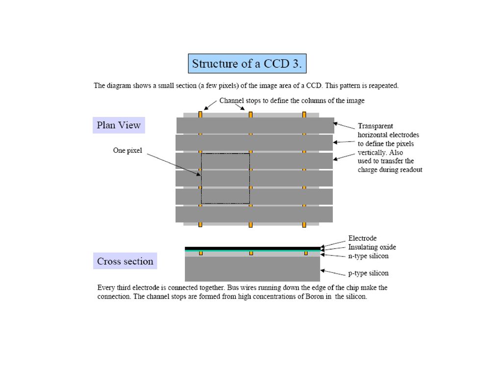
CCD 기본 Two –dimensional array of thousands to millions of metal insulator semiconductor (MIS) photosensitive capacitors(금속절연 반도체 감광 캐패시터 )(called picture elements or pixels) charge storage Typical : 2K * 2K (15mm * 15 mm) size 30mm *30mm Pixels are interconnected in such a way that their stored charges can flow from pixel to pixel as voltages are changed in a systematic way. charge transfer
 photosensitive capacitors(금속절연 반도체 감광 캐패시터 )(called picture elements or pixels) charge storage. Typical : 2K * 2K (15mm * 15 mm) size 30mm *30mm. Pixels are interconnected in such a way that their stored charges can flow from pixel to pixel as voltages are changed in a systematic way. charge transfer.")
12
A wafer is a thin slice of semiconductor material, such as a silicon crystal, used in the fabrication of integrated circuits and other microdevices. The wafer serves as the substrate for microelectronic devices built in and over the wafer and undergoes many microfabrication process steps such as doping or ion implantation, etching, deposition of various materials, and photolithographic patterning

14
CCD 구조 Silicon substrate =260 mm 두께 (doped with phosphorus impurities to make a p-type semiconductor) impurity phosphorus (fixed negative charge), upper part (2mm);doped with boron(n-type semiconductor= fixed positive charges) & charge density 100 higher than p-type silicon
;doped with boron(n-type semiconductor= fixed positive charges) & charge density 100 higher than p-type silicon.")
28
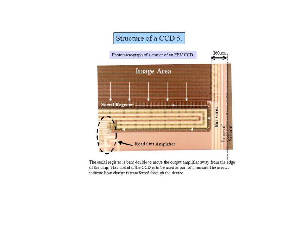
Read out Readout

29
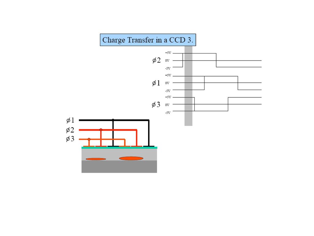
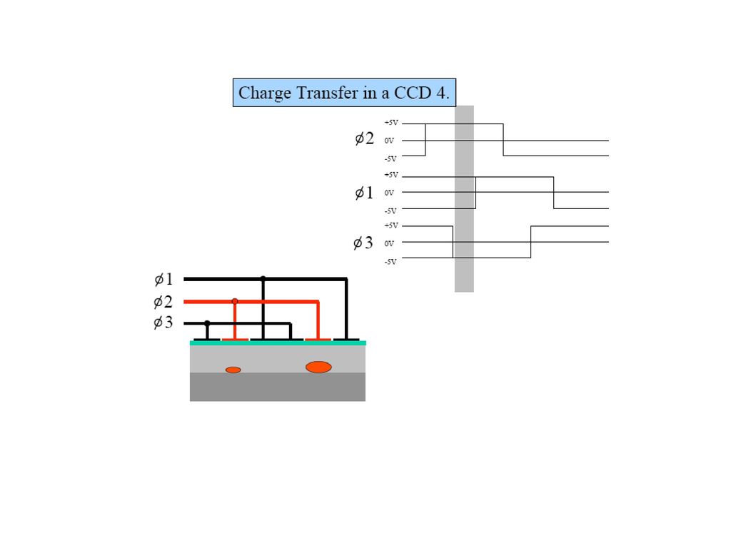
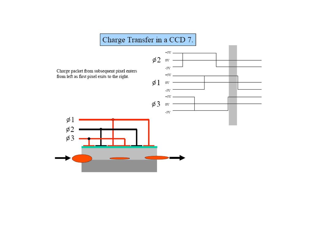
전하 전달 CCD 에 쪼여진 광자가 device 내에 생성한 전자와 구멍(positive charge)쌍에서 전자를 MIS capacitor에 저장 이를 serial 식으로 읽어(readout) :”water bucket 개념
 : water bucket 개념.")
34
파장에 따른 CCD 특성 Out side of 3500A, over 8000A : 1. 광자가 silicon을 통과하거나
2. thin surface layers or gate structure에 흡수 3. simply reflect off the CCD surface 그림 : 파장에 따른 광자가 silicon 에 흡수(63%=1/e) 되는 길이
 되는 길이.")
35
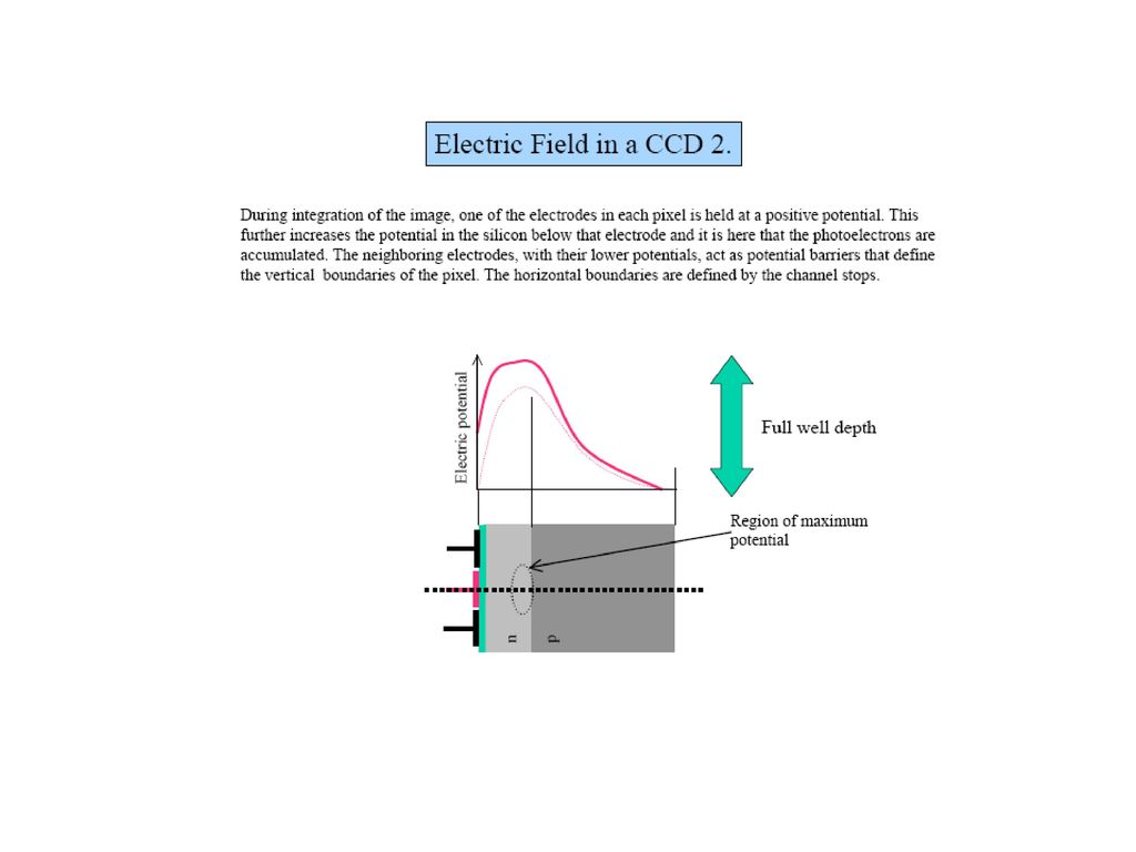
CCD 개념 입사 광자(1.1- 4ev A-3000A) 가 pixel에 silicon substrate (band gap energy 1.14 ev) 에 쪼이면 흡수되어 광전효과 또는 crystal 면의 열적 요동으로 silicon의 valence 전자가 떨어져 conduction band 로 올라가 자유로이 움직인다. 즉 electron-hole pair가 형성. 이 자유 전자는 100 m초 이후 다시 valence 전자로 돌아가므로 impurity로 silicon을 doped하고 positive voltage(10ev) 를 걸어 positive hole을 제거하여 depletion region을 만들어, 만들어진 전자만 남게 한다. 이 depletion region 에 축적될 수 있는 전자의 최대 수가 제한되므로 이를 full well capacity 라 하며 전형적으로 수 만개가 된다. 실제 silicon은 1.1ev(근적외선) 에서 10ev(soft X-ray) 까지 광전효과를 갖음 Thermal agitation : dark current ~ exp (-B/kT) , B constant cooling -80 ~ -100 도 : dark 무시
 가 pixel에 silicon substrate (band gap energy 1.14 ev) 에 쪼이면 흡수되어 광전효과 또는 crystal 면의 열적 요동으로 silicon의 valence 전자가 떨어져 conduction band 로 올라가 자유로이 움직인다. 즉 electron-hole pair가 형성. 이 자유 전자는 100 m초 이후 다시 valence 전자로 돌아가므로 impurity로 silicon을 doped하고 positive voltage(10ev) 를 걸어 positive hole을 제거하여 depletion region을 만들어, 만들어진 전자만 남게 한다. 이 depletion region 에 축적될 수 있는 전자의 최대 수가 제한되므로 이를 full well capacity 라 하며 전형적으로 수 만개가 된다. 실제 silicon은 1.1ev(근적외선) 에서 10ev(soft X-ray) 까지 광전효과를 갖음. Thermal agitation : dark current ~ exp (-B/kT) , B constant cooling -80 ~ -100 도 : dark 무시.")
36
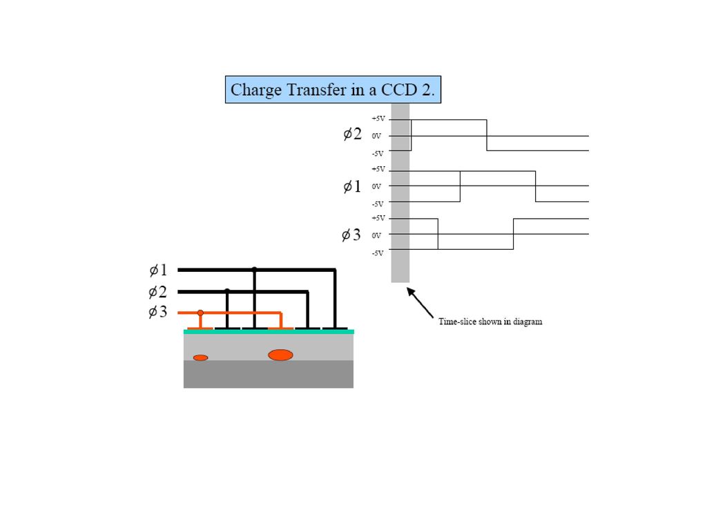
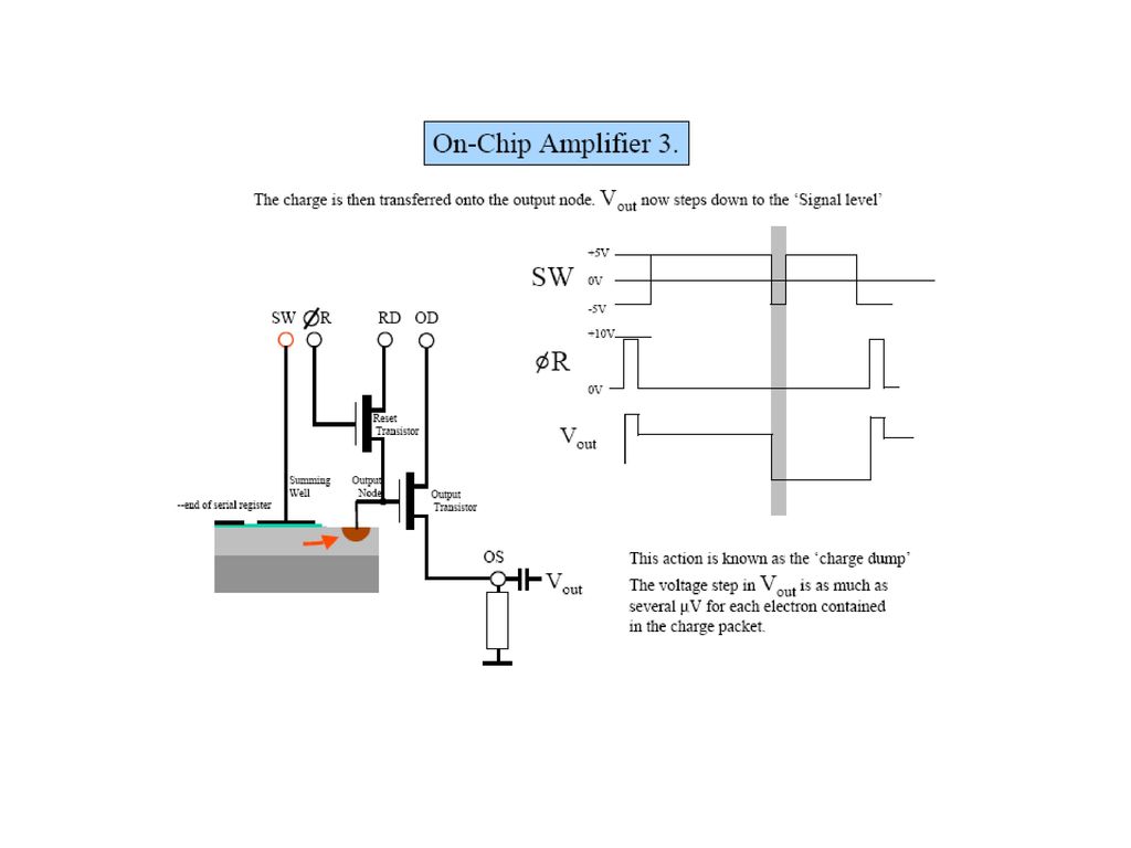
Gates 들이 충분히 접해 있어 (charged coupled라는 이름이 유래됨) depletion region에 전자는 gate의 electric voltage depth를 조절하여 transport 전형적인 CCD 는 3gates-3phase device(0,5,10 V) : clocking the device allow charge shifted in a serial fasion charge transfer efficiency (CTE) = (99.999%) 한 Column 이 readout register에 오면 그중 하나가 on-chip amplfier로 가서 전하가 voltage로 전환되어 이것은 더욱 증폭된 뒤에 analog-to –digital converter 에 의해 digital 자료가 입력 된다. 전형 적이 AD converter 12, 14, 16 bits 로 4096, 16,384, 65,536 분에 1의 정확성을 갖는다. ADU (analog to digital Unit) Gain = the amount of voltage needed to produce 1 ADU 예 : gain = 10 electrons / ADU
 : clocking the device. allow charge shifted in a serial fasion. charge transfer efficiency (CTE) = (99.999%) 한 Column 이 readout register에 오면 그중 하나가 on-chip amplfier로 가서 전하가 voltage로 전환되어 이것은 더욱 증폭된 뒤에 analog-to –digital converter 에 의해 digital 자료가 입력 된다. 전형 적이 AD converter 12, 14, 16 bits 로 4096, 16,384, 65,536 분에 1의 정확성을 갖는다. ADU (analog to digital Unit) Gain = the amount of voltage needed to produce 1 ADU. 예 : gain = 10 electrons / ADU.")
37
파장에 따른 광전효율

41
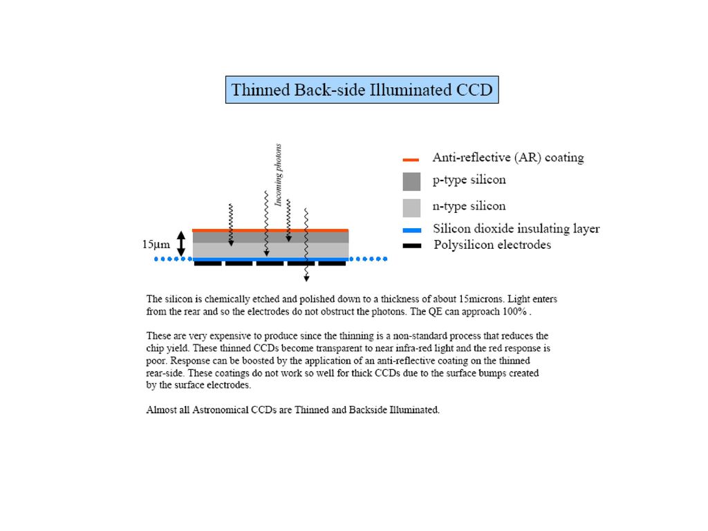
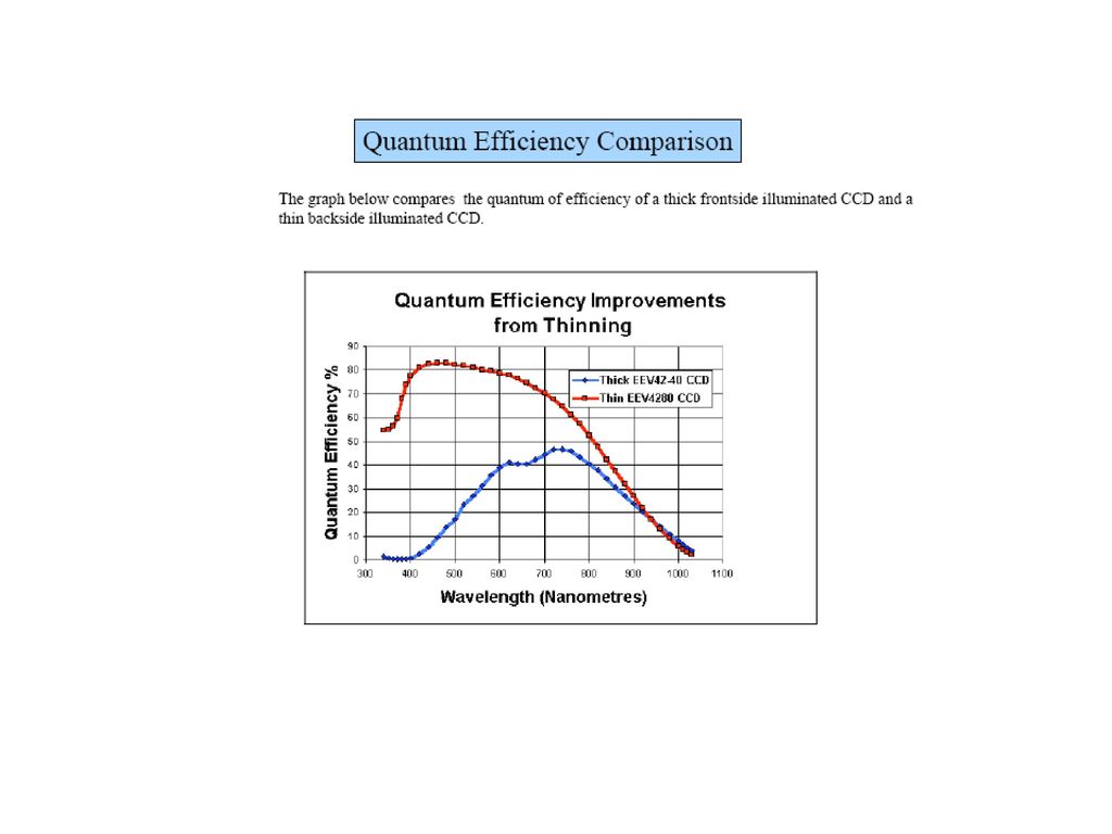
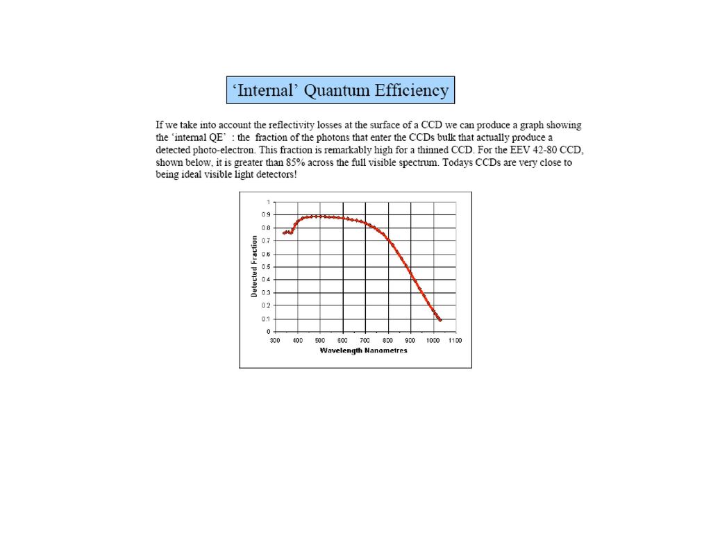
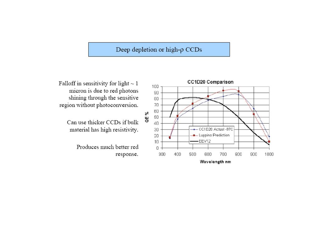
CCD의 기본 개념 Light sensitive silicon chip = large numbers of pixels (picture elements) Pixel size = ~ mm 광자 효율(Quantum efficiency) ; =detected photons by CCD / falling photons on CCD = S/N ratio of input and detected signal photon noise 가 중요한 noise S/N 파장의 함수 초기 CCD (Fairchild or GEC) : peak 40%, now :peak near 90%, but > 60% over 2/3 of spectral range (cf :사진 2% (kodak IIIaJ 3%), hypersensitized 10%, : solid-state imaging device 20-30%) Thick chip = frontside illuminated chips : light passes through some of the electronic layers of the CCD before hitting the silicon detecting level Low QE in the blue since electronic layers absorb much of the blue light Thin chip=backside illuminated : the silicon layer is mechanically or chemically thinned and the light enters the silicon directly Better blue QE Thin chip and thick chip have more similar red QE, but the thin chips usually have higher QE at all wavelengths than the thick chip
![]()
52
Charged Coupled Device
장점 : 1. 높은 양자효율 (60-80%) (사진 :2-10%, PMT: 20-40%) 2. 선형 반응 (사진=특성곡선) 3. digital 정보 (사진 =아날로그) 콤퓨터 영상처리 4. 이차원 : 측광 및 측성 (PMT =측광 only) 5. 넓은 다이나마익 범위 > 10등급 이상 (사진=5등급) 6. 넓은 파장 영역에 반응 (사진 =특수처리 spectral sensitization) 단점 : 1. 좁은 시야 (망원경시야 >> CCD에 의해 제한된 시야) 2. 엄청난 자료 (512*512 CCD = 262,144 pixels, 4K*4K = 4096*4096 = 16,777,216 pixels) 3. 각 pixel의 다른 반응 : flat 보정 필수 4. readout 잡음 관측된 자료를 읽어 올 때 발생 5. RN 잡음을 포함한 잡음을 줄이기 위한 냉각 (-100도 C ) 필수
 (사진 :2-10%, PMT: 20-40%) 2. 선형 반응 (사진=특성곡선) 3. digital 정보 (사진 =아날로그) 콤퓨터 영상처리. 4. 이차원 : 측광 및 측성 (PMT =측광 only) 5. 넓은 다이나마익 범위 > 10등급 이상 (사진=5등급) 6. 넓은 파장 영역에 반응 (사진 =특수처리 spectral sensitization) 단점 : 1. 좁은 시야 (망원경시야 >> CCD에 의해 제한된 시야) 2. 엄청난 자료 (512*512 CCD = 262,144 pixels, 4K*4K = 4096*4096 = 16,777,216 pixels) 3. 각 pixel의 다른 반응 : flat 보정 필수. 4. readout 잡음 관측된 자료를 읽어 올 때 발생. 5. RN 잡음을 포함한 잡음을 줄이기 위한 냉각 (-100도 C ) 필수.")
53
검출기들의 양자효율

63
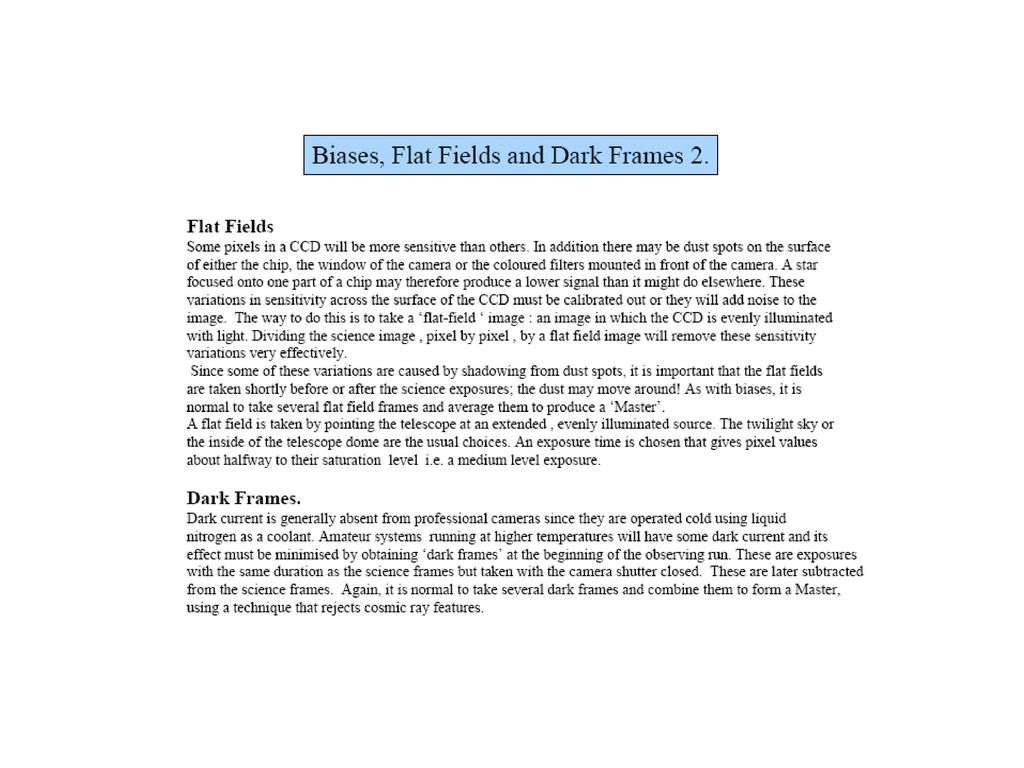
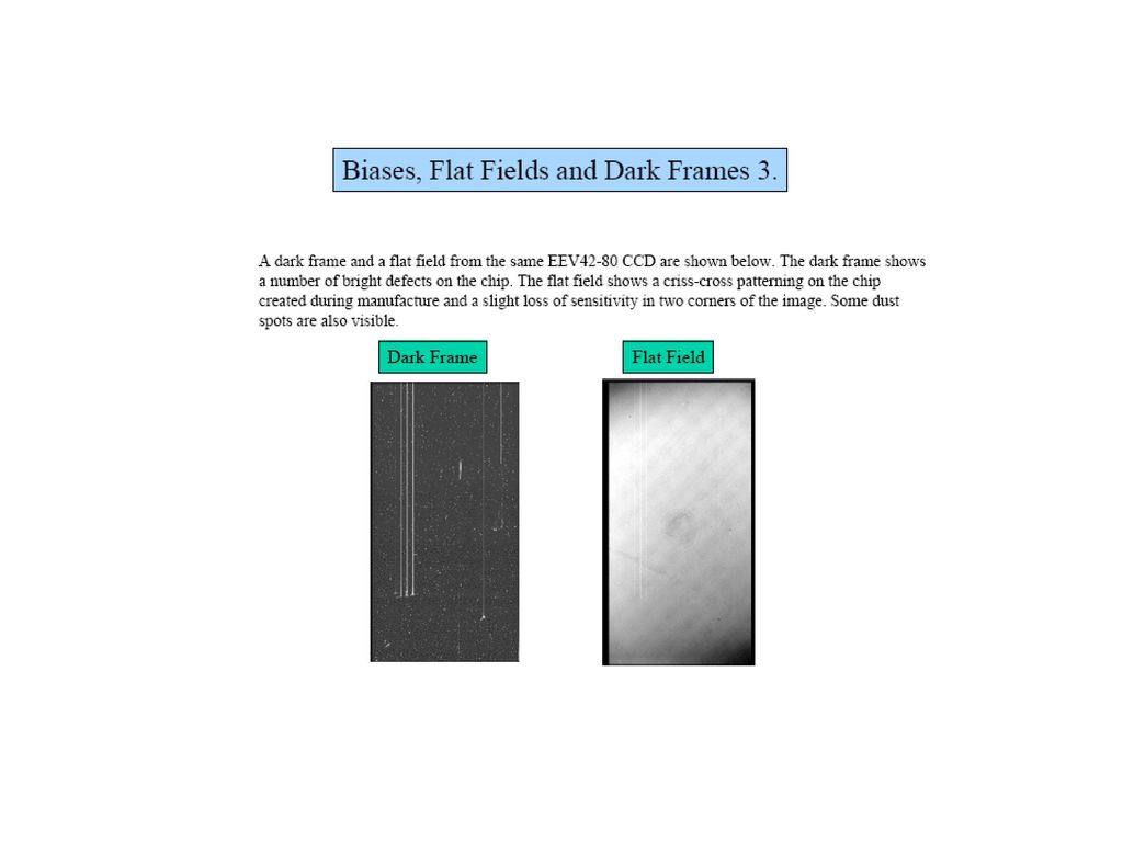
CCD 측정 CCD counts : bias + dark current + signal related to the number of electrons liberated by photons in each pixel Only fraction of photons generate electrons ; QE Photons = number of electrons (bias & dark removed) /QE = gain * DN / QE CCD = integrating device is controlled by a mechanical shutter or electrically( changing voltages in CCD) READ NOISE : on-chip amps average noise per pixel = read noise : electrons per pixel per read out (same whether exp 0.1 or 3 hours) Bias frame :simply read out zero image = bias signal changing with changing CCD Temp, also with read noise Dark frame : Without any light, signal caused by thermal excitation of electrons in the CCD : very sensitive to Temp cooling
![]()
64
CCD 측정 –cont Flat frame : uniformly illuminating the CCD will NOT generate an equal signal in each pixel ; small scale (pixel to pixel) sensitivity variation : caused by slight differences in pixel sizes Large scale (over large fraction of chip) sensitivity variation : by small variations in the silicon thickness across the chip These can be up to 10% variations over the chip Data frames : Exp time for best S/N Signal =photons “root N” noise ; no way to get rid of this noise : poisson noise Dark noise, read out noise, cosmic ray
![]()
65
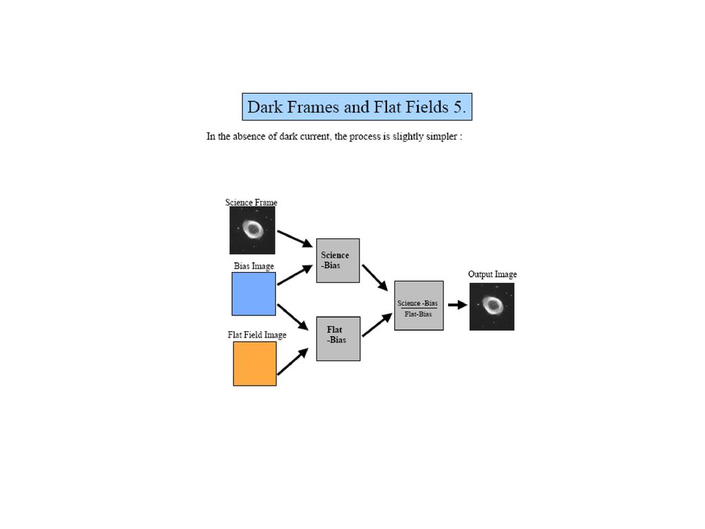
CCD 관측 1. a number of bias frames - median combine to a single low noise bias frame 2. a number of dark frames – no light, finite integration time equal to the data frame integration) , combine dark frames into a single low-noise frame (after subtracting bias frames) 3. a number of flat frames in each filter – twilight sky , dome flat (bias, dark subtracted) normalize the flat so that the average signal in each pixel is 1.00 ( simply by dividing by the average signal) 4. subtract low-noise bias frame and low-noise dark frame from object frame. Then, divide this by the normalized frame Reduction frame =[(row-object frame)-(low-noise bias frame)-(low-noise dark frame)]/(normalized flat frame)] Amateur : CCD C below the ambient T (0 to -40 C) dark : changes in the dark – source of problems take darks before and after object, these averaged and subtracted from the data frames (here dark really “dark+bias”) inefficient at using telescope time – much used to dark frames
 , combine dark frames into a single low-noise frame (after subtracting bias frames) 3. a number of flat frames in each filter – twilight sky , dome flat (bias, dark subtracted) normalize the flat so that the average signal in each pixel is 1.00 ( simply by dividing by the average signal) 4. subtract low-noise bias frame and low-noise dark frame from object frame. Then, divide this by the normalized frame. Reduction frame =[(row-object frame)-(low-noise bias frame)-(low-noise dark frame)]/(normalized flat frame)] Amateur : CCD C below the ambient T (0 to -40 C) dark : changes in the dark – source of problems. take darks before and after object, these averaged and subtracted from the data frames (here dark really dark+bias ) inefficient at using telescope time – much used to dark frames.")
76
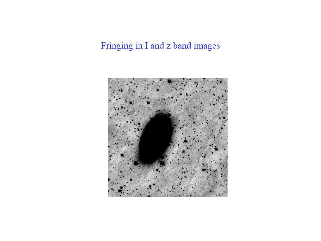
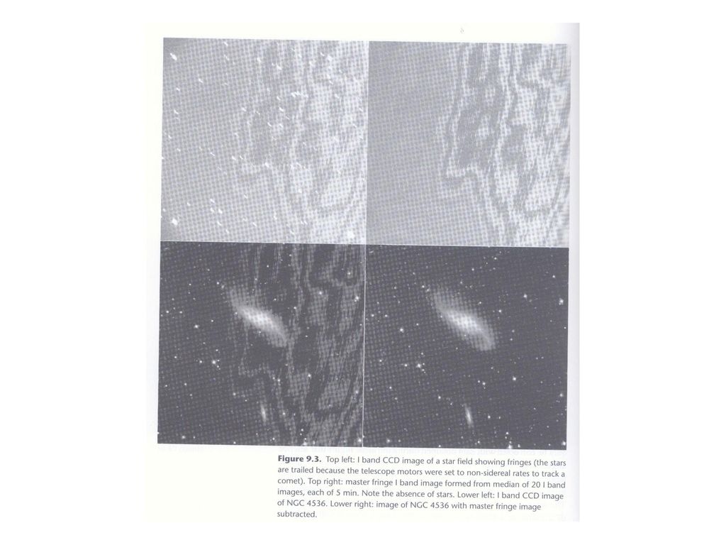
Night sky emission lines produce fringes on a CCD image; also additive noise ;
usually in near IR I, Z bands : observe the sparse field with the same exp of the targets

77
SKY BACKGROUND Shows red continuum, Hg, and Na emission lines from scattered city lights. (HPS = “high pressure sodium” lamps). Strong [O I] lines are auroral. Region redward of 6200 °A shows start of forest of upper-atmospheric OH lines, which continues through near-IR.
. Strong [O I] lines are auroral. Region redward of 6200 °A shows start of forest of upper-atmospheric OH lines, which continues through near-IR.")
78
SKY BACKGROUND Night sky emission lines (mainly OH), near-IR Shows continuation of atmospheric OH spectrum from preceding KPNO plot. OH forms at 75 km altitude, so affects all ground-based sites. Impact of lines I devastating for certain kinds of observations. Natural extra-atmospheric background at these wavelengths is up to 1000 times fainter.
, near-IR Shows continuation of atmospheric OH spectrum from preceding KPNO plot. OH forms at 75 km altitude, so affects all ground-based sites. Impact of lines I devastating for certain kinds of observations. Natural extra-atmospheric background at these wavelengths is up to 1000 times fainter.")
86
Mosaic CCD

Similar presentations


. Carbon nanotube( 탄소 나노튜브 ) Multi-walled carbon nanotube.>")


 23.1 전하의 특성 23.2 유도에 의해 대전된 물체 23.3 쿨롱의 법칙>")


 2008.10.28 박사 과정 이종환 011.9640.5025 leejh@astro.snu.ac.kr.>")


.>")
