Download presentation
Presentation is loading. Please wait.

1
Chapter 7 Ion Implantation.
7.1 Range of Implanted Ions. 7.2 Implant Damage and Annealing. 7.3 Implantation-Related Processes. 7.4 Ion Implantation Simulation. 7.5 Summary.

2
7.1 Range of Implanted Ions.
• Ion implantation; the introduction of energetic, charged particles into a substrate such as silicon. • Implantation energies; 1keV ~ 1 MeV. average depths ranging from 10nm to 10㎛. • Ion doses vary from 1012ions/cm2 for threshold voltage adjustment to 1018ions/cm2 for the formation of buried insulating layers. • main advantages; more precise control and reproducibility of impurity dopings. lower processing temperature compared with those of the diffusion process.

3
Figure 7.1 Comparison of (a) diffusion and (b) ion-implantation techniques
for the selective introduction of dopants into the semiconductor substrate.

4
• ion source; a break up source gases such as BF3 or AsH3 into charged
ions (B+ or As+). • Mass spectrometer; 입자의 운동은 원. 원심력과 balance되어야 함. • High-voltage accelerator; beam에 energy를 보탠다. high voltage, x-ray emission으로 부터 보호하기 위하여 ion source와 accelerator는 protective shield 내부에 설치. ; dc전류를 변화시키면 ion species를 선택.
. • Mass spectrometer; 입자의 운동은 원. 원심력과 balance되어야 함. • High-voltage accelerator; beam에 energy를 보탠다. high voltage, x-ray emission으로 부터 보호하기 위하여 ion source와. accelerator는 protective shield 내부에 설치. ; dc전류를 변화시키면 ion species를 선택.")
5
• scanning system. x-, y-axis deflection plate (편향판). beam을 약간 꾸부림; 중성입자가 target에 hit하는 것을 막는다. target chamber. - Si wafer가 target. - target area는 ground potential을 유지; safety. • implantor에서 압력; 10-4Pa 이하, gas 분자에 의한 ion scattering을 최소화 하기 위하여. • the energetic ions lose energy through collisions with electrons and nuclei in the substrate and finally come to rest at some depth within the lattice. • damage of the semiconductor lattice due to ion collisions. ; annealing treatment가 필요하다.

6
7.1.1 Ion Distribution. • projected range (Rp)
; ion이 stop하기 전 travel한 평균거리. • projected straggle( ) ; statistical fluctuations in the projected range. • lateral straggle( ) ; statistical fluctuation along an axis perpen- dicular to the axid of incidence. • implanted impurity profile; Gaussian 분포함수. S; ion dose per unit area. ion 농도; Figure 7.3 (a) Schematic of the ion range R and projected range Rp. (b) Two-dimensional distribution of the implanted icons.
 ; statistical fluctuations in the projected. range. • lateral straggle( ) ; statistical fluctuation along an axis perpen- dicular to the axid of incidence. • implanted impurity profile; Gaussian 분포함수. S; ion dose per unit area. ion 농도; Figure 7.3. (a) Schematic of the ion range R and projected range Rp. (b) Two-dimensional distribution of the implanted icons.")
7
7.1.2 Ion stopping. • two stopping mechanisms.
첫째; ion의 energy를 target nuclei로 transfer에 의하여 incident ion의 편향과, 많은 target nuclei를 원래 lattice site로 부터 옮아 가게 한다. nuclear stopping power 둘째; - interaction of the incident ion with the cloud of electrons surrounding the target’s atoms (coulombic interaction). - electron이 excitation 혹은 atom 으로 부터 ejection (ionization) 될 수 있다. - electronic stopping power • 거리에 대하여 energy 손실의 평균율은,
. - electron이 excitation 혹은 atom 으로 부터 ejection (ionization) 될 수. 있다. - electronic stopping power. • 거리에 대하여 energy 손실의 평균율은,")
8
• the total distance traveled by the ion before coming to rest (R),
E0; initial ion energy. • nuclear stopping. 탄성 충돌에서 incident particle M1에서 energy 손실 혹은 M2로 전달 된 energy. Nuclear stopping power는 low energy에서는 선형으로 증가, 그리고 Sn(E)는 최대 값에 도달 한다. High energy에서는 작아진다. 빠른 입자들이 충분한 충돌 시간을 가지지 못하기 때문이다 (Fig7.5). 보다 무거운 원자 (예As)는 보다 큰 nuclear stopping power를 가진다. 즉 단위 거리당 보다 큰 energy 손실을 가진다. Figure Collision of hard spheres.
는 최대 값에 도달. 한다. High energy에서는 작아진다. 빠른 입자들이 충분한 충돌 시간을 가지지 못하기. 때문이다 (Fig7.5). 보다 무거운 원자 (예As)는 보다 큰 nuclear. stopping power를 가진다. 즉 단위 거리당 보다. 큰 energy 손실을 가진다. Figure 7.4 Collision of hard spheres.")
9
Figure Nuclear stopping power, Sn(E) and electronic stopping power, Se(E) for As, P, and B in Si. The points of intersection of the curves correspond to the energy at which nuclear and electronic stopping are equal.

10
• electronic stopping. incident ion의 velocity에 비례한다 (Fig 7.5). ; relatively weak function of atom mass and atomic number. • Fig 7.5에서 crossover energies [Se(E)=Sn(E)]. B인 경우, target silicon atom에 대하여, crossover energy가 10keV이다. 이것은 implantation energy가 1keV ~ 1MeV이므로 주요 에너지 손실 mechanism은 electronic stopping이다. As인 경우 crossover energy가 700keV이므로 nuclear stopping이 dominant 하다. P인 경우, crossover energy가 130keV이므로 130keV의 E0에서는 nuclear stopping, 그 이상의 E0에서는 electronic stopping이 일어난다.
=Sn(E)]. B인 경우, target silicon atom에 대하여, crossover energy가 10keV이다. 이것은 implantation energy가 1keV ~ 1MeV이므로 주요 에너지 손실. mechanism은 electronic stopping이다. As인 경우 crossover energy가 700keV이므로 nuclear stopping이 dominant. 하다. P인 경우, crossover energy가 130keV이므로 130keV의 E0에서는 nuclear. stopping, 그 이상의 E0에서는 electronic stopping이 일어난다.")
11
• approximate equations,
Figure Projected range, projected straggle, and lateral straggle for (a) B, P, and As in silicon and (b) H, Zn, and Te in gallium arsenide.
 B, P, and As in silicon and (b) H, Zn, and Te in gallium arsenide.")
12
7.1.3 Ion channeling. • Gaussian 분포의 projected range 그리고 straggle은 amorphous 혹은 fine- grain polycrystalline substrate에서 implanted ions의 good description이다. • ion channeling. if the ion beam is aligned along a crystal axis, there can be much deeper penetration. energy loss mechanism은 electron stopping이다. Figure Model for a diamond structure , viewed along a <110> axis.

13
• 그림에서 exponetial tail은 ion channeling effect이다.
<111> <100> <110> Figure Impurity profile obtained in a purposely misoriented target. Ion beam is incident 7°C from the <111> axis.

14
• channeling을 최소화 하는 방법 (Fig 7.9).
blocking amorphous surface layer; thin layer of grown silicon dioxider. misorientation of the wafer; 5° ~10° of the major plane. creating a damaged layer in the wafer surface. Figure 7.9 Minimizing channeling. Implantation through an amorphous oxide layer. Misorientation of the beam direction to all crystal axes. (c) Pre-damage on the crystal surfaces.
 Pre-damage on the crystal surfaces.")
15
7.2 Implant Damage and Annealing.
• lattice disorder; nuclear collision에 의하여 host atom이 변위 되었을 때. • 단위 체적당 displaced atom 들이 반도체의 atomic density에 근접할 때, material은 amorphous가 된다. • light ion (예 B+ in silicon)에 대한 energy loss는 electronic collisions (Fig 7.5 참조) 때문이며, ion들은 기판 깊숙이 들어간다. ion energy가 crossover energy (10keV for boron) 이하로 줄어들면, nuclear stopping이 우세하게 된다. 그러므로 lattice disorder의 대부분은 final ion position에서 일어난다 (Fig 7.10 a). (예) 100keV boron ion에 대하여, Rp=0.31㎛ (Fig 6 a 에 의하여). initial nuclear energy loss=3eV/Å (Fig 7.5에 의하여).
에 대한 energy loss는 electronic collisions. (Fig 7.5 참조) 때문이며, ion들은 기판 깊숙이 들어간다. ion energy가 crossover energy (10keV for boron) 이하로 줄어들면, nuclear stopping이 우세하게 된다. 그러므로 lattice disorder의 대부분은. final ion position에서 일어난다 (Fig 7.10 a). (예) 100keV boron ion에 대하여, Rp=0.31㎛ (Fig 6 a 에 의하여). initial nuclear energy loss=3eV/Å (Fig 7.5에 의하여).")
16
Si에서 lattice plane 사이 spacing이 2.5Å 이므로 각 lattice plane 에서 7.5eV를
잃는다. Si atom을 변위 시키는 데는 15eV이 필요하므로, Si atom을 변위 시키지 못한다. 50keV (1500Å의 depth에서)으로 줄어들면, nuclear stopping에 의한 energy 손실은 각 lattice plan에 대하여 15eV(6eV/Å)이며, lattice disorder를 발생 시 킬 수 있다. lattice plane 당 1 atom이 변위 되었다면 600 lattice atom이 변위 (즉 1500Å/ 2.5Å)된다. 만약 atom이 original position으로 부터 대략 25Å 움직였다면 damage volume은 Å Å damage density는 이것은 atom들의 0.4%이다. 그러므로 amorphous layer를 발생 시키기 위하여 high ion의 very high close가 필요하다.
으로 줄어들면, nuclear stopping에 의한 energy. 손실은 각 lattice plan에 대하여 15eV(6eV/Å)이며, lattice disorder를 발생 시. 킬 수 있다. lattice plane 당 1 atom이 변위 되었다면 600 lattice atom이 변위 (즉 1500Å/ 2.5Å)된다. 만약 atom이 original position으로 부터 대략 25Å 움직였다면. damage volume은 Å Å. damage density는 이것은 atom들의 0.4%이다. 그러므로. amorphous layer를 발생 시키기 위하여 high ion의 very high close가 필요하다.")
17
• heavy ion 들에 대하여, energy loss는 주로 핵 충돌에 의한다.
그러므로 상당한 damage를 기대 할 수 있다. (예) 100ke Vs ion. Rp=0.006㎛ 혹은 60nm. 평균 핵 energy 손실은 1320eV/nm (Fig 7.5). As ion은 각 lattice plane 당 330eV (132eV/Å×2.5Å) 잃는다. energy의 대부분은 한 개의 primary silicon atom에 주어진다. 각 primary atom은 22 displaced target atoms (330eV/15eV)을 야기 시킨다. displaced atoms의 total number는 5280이다. (1320eV/nm × 60nm ÷15eV = 5280). displaced atom에 대하여 25Å의 range라고 가정하면 damage volume은 damage density는 atom의 total number의 약 10%이다. heavy-ion implantation의 결과로서, material은 기본적으로 amorphous가 된다 (Fig 7.10 b). .
 100ke Vs ion. Rp=0.006㎛ 혹은 60nm. 평균 핵 energy 손실은 1320eV/nm (Fig 7.5). As ion은 각 lattice plane 당 330eV (132eV/Å×2.5Å) 잃는다. energy의 대부분은 한 개의 primary silicon atom에 주어진다. 각 primary. atom은 22 displaced target atoms (330eV/15eV)을 야기 시킨다. displaced atoms의 total number는 5280이다. (1320eV/nm × 60nm ÷15eV = 5280). displaced atom에 대하여 25Å의 range라고 가정하면 damage volume은. damage density는 atom의 total number의 약 10%이다. heavy-ion implantation의 결과로서, material은 기본적으로 amorphous가. 된다 (Fig 7.10 b). .")
18
Figure 7.10 Implantation disorder caused by (a) light ions and (b) heavy ions.
 light ions and (b) heavy ions.")
19
• crystalline material을 amorphous form으로 바꾸는데 요구되는 dose량 추정
하기, energy density는 물질을 용융하는데 필요한 energy (i.e., 1021keV/cm3) 정도의 크기로 한다. 100keV-As ion에 대하여 amorphous silicon을 만드는데 필요한 dose, 100keV boron ions에 대하여 요구되는 dose는 3×10¹⁴ions/cm2 (Boron은 Arsenic 보다 Rp가 5배 크다). 그러나 실제로는 higher doses ( >1016ions/cm2)가 room temperature에서 boron implantation에서 요구된다. 왜냐하면, ion path 따라 damage의 nonuniform distribution 때문이다.
 정도의 크기로 한다. 100keV-As ion에 대하여 amorphous silicon을 만드는데 필요한 dose, 100keV boron ions에 대하여 요구되는 dose는 3×10¹⁴ions/cm2. (Boron은 Arsenic 보다 Rp가 5배 크다). 그러나 실제로는 higher doses ( >1016ions/cm2)가 room temperature에서. boron implantation에서 요구된다. 왜냐하면, ion path 따라 damage의 nonuniform distribution 때문이다.")
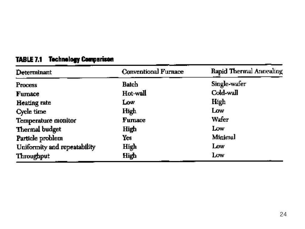
20
7.2.2 Annealing. • ion implantation 으로 부터 오는 damaged region 그리고 disorder cluster 때문에 mobility 와 lifetime과 같은 반도체 parameter들이 심각하게 퇴화된다. • implanted 된 ion들의 대부분이 substitutional sites에 위치하고 있지 않다. • implanted ion 들을 활성화 시키기 위하여, 그리고 mobility와 다른 물질 parameter를 원상 회복 시키기 위하여, 반도체를 적당한 온도와 시간을 조합하여 annealing 하여야 한다. • conventional annealing; open-tube, batch furnace system similar to that used for thermal oxidation. long time, high temperature. • Rapid-thermal annealing.

21
Conventional Annealing of Boron and Phosphorus.
Figure 7.11 Annealing temperature versus dose for 90% activation of boron and phosphorus.

22
• 주어진 ion dose에서, 30분 annealing에 의하여 implanted ion의 90%가 activated
되는 온도로서 annealing temperature를 정의. • Boron; higher dose에 대하여 higher annealing temperature. • phosphorus; lower dose 에서는 annealing behavior가 Boron과 같은 비슷한 모양이다. 그러나 dose가 1015cm-2에서 annealing temperature가 600℃이하로 떨어진다. 이러한 현상은 solid-phase epitaxy process(8장 참조)와 관계 있다. 6×1014cm-2 보다 더 큰 phosphorus dose에서 silicon surface layer는 amorphous가 된다. • amorphous layer 바로 밑에 있는 single-crystal semiconductor는 amorphous layer의 재결정화를 위한 seed로서 작용한다. <100>방향 따라 epitaxial growth rate는 activation energy 2.4eV로써 550℃에서 10nm/min, 600℃에서 50nm/min이다. 그러므로 100 ~ 500nm amorphous layer는 몇 분 안에 재 결정화 될 수 있다.
와 관계 있다. 6×1014cm-2 보다 더 큰 phosphorus dose에서 silicon surface. layer는 amorphous가 된다. • amorphous layer 바로 밑에 있는 single-crystal semiconductor는 amorphous. layer의 재결정화를 위한 seed로서 작용한다. <100>방향 따라 epitaxial growth. rate는 activation energy 2.4eV로써 550℃에서 10nm/min, 600℃에서. 50nm/min이다. 그러므로 100 ~ 500nm amorphous layer는 몇 분 안에 재 결정화. 될 수 있다.")
23
Rapid Thermal Annealing
• heated wafer로부터 측정된 온도는 보통 600℃로부터 1100℃. • a wafer is heated quickly under atmospheric conditions or at low pressure under isothermal conditions. • tungsten filament 혹은 arc lamps. chamber : quartz, silicon carbide, stainless steel, aluminum. quartz windows (optical radiation을 위하여), computer control, noncontact optical pyrometer. Figure Rapid thermal annealing system that is optically heated.
, computer control, noncontact optical pyrometer. Figure 7.12 Rapid thermal annealing system that is optically heated.")
25
7.3. Implantation-Related Processes.
Multiple Implantation and Masking. Figure 7.13 Composite doping profile using multiples implants. Figure 7.14 Minimum thickness of SiO2 (——), Si3N4 ( ), and a photoresist (-•-•-•-) to produce a masking effectiveness of 99.99%.
, Si3N4 ( ), and a photoresist (-•-•-•-) to produce a masking effectiveness. of 99.99%.")
26
• depth d를 넘은 영역에서 implanted dose (shown shaded).
(9) (10) • Table 6.1로 부터 • depth d를 넘어가는 dose의 비는 transmission coefficient (T)로 나타낸다. (11) • incident ion의 99.99%를 stop하기 위한 d의 값 (T=10-4)이 Fig 7.14에서 보인다. ※ 식비의 근사 식 T = 10-4 될 때 u = 2.8 .
 (10) • Table 6.1로 부터. • depth d를 넘어가는 dose의 비는 transmission coefficient (T)로 나타낸다. (11) • incident ion의 99.99%를 stop하기 위한 d의 값 (T=10-4)이 Fig 7.14에서 보인다. ※ 식비의 근사 식. T = 10-4 될 때 u =")
27
7.3.2 Tilt-Angle Ion Implantation.
Figure (p. 139) 60-keV arsenic implanted into silicon, as a function of beam tilt angle. Inset shows the shadow area for tilt-angle ion implantation. • tilt-angle ion implantation에서 shadow effect를 고려하여야 한다. patterned mask의 높이가 0.5㎛ 이라면, 7° incident ion beam이 61nm shadow를 유발 시킨다.
 60-keV arsenic implanted into silicon, as a function of beam tilt angle. Inset shows the shadow area for tilt-angle ion implantation. • tilt-angle ion implantation에서 shadow effect를 고려하여야 한다. patterned mask의 높이가 0.5㎛ 이라면, 7° incident ion beam이 61nm. shadow를 유발 시킨다.")
28
7.3.3 High Energy and High-current Implantation.
• High-energy implantor; 1.5 ~ 5MeV. • High temperature에서 long diffusion 없이 수 micrometer의 깊이로 doping. • low-resistivity buried layer (CMOS device를 위하여 surface 아래 1.5 ~3.0 ㎛ 정도)를 만든다. • High-current implantor (10 ~20 mA, 25 ~ 30keV에서 동작). ; predeposition step (in diffusion 기술)을 위하여 사용. • threshold voltage adjustment (in MOS devices). • SIMOX; separation by implantation of oxygen. Figure Threshold voltage adjustment using boron ion implantation.
를 만든다. • High-current implantor (10 ~20 mA, 25 ~ 30keV에서 동작). ; predeposition step (in diffusion 기술)을 위하여 사용. • threshold voltage adjustment (in MOS devices). • SIMOX; separation by implantation of oxygen. Figure 7.16 Threshold voltage adjustment. using boron ion implantation.")
Similar presentations


. Carbon nanotube( 탄소 나노튜브 ) Multi-walled carbon nanotube.>")
 2008.01.08 Joo Suk-bae. 회절 (Diffraction) 입자의 진행경로에 틈이 있는 장애물이 있으면 입자는 그 틈을 지나 직선으로 진행한다. 이와 달 리 파동의 경우, 틈을 지나는 직선 경로뿐 아니라 그 주변의.>")
 1.CVD(Chemical Vapor Deposition), 화학기상증착 기술이란 ? 먼저 CVD 기술을 이해하기 전에 CVD 기술이 반도체 제조공정 중 어디에 위치하고 어떻게 사용되는지를.>")


>")


